Everything You Always Wanted to Know About SDRAM (Memory): But Were Afraid to Ask
by Rajinder Gill on August 15, 2010 10:59 PM ESTEvery read/write memory transaction can be segmented by type into one of three performance bins depending on the status of the bank/page to be accessed. These bins, in order of best to worst, are page-hit, page-empty, and page-miss. For the most part, anything we can do to increase the number of page-hit transactions or reduce the number of page-miss transactions is a good thing.
A page-hit access is defined as any read or write operation to an open page. That is, the bank containing the open page is already active and is immediately ready to service requests. Because the target page is already open, the nominal access latency for any memory transaction falling into this category is approximately tCAS (the CAS Latency of the device).
Click to enlarge
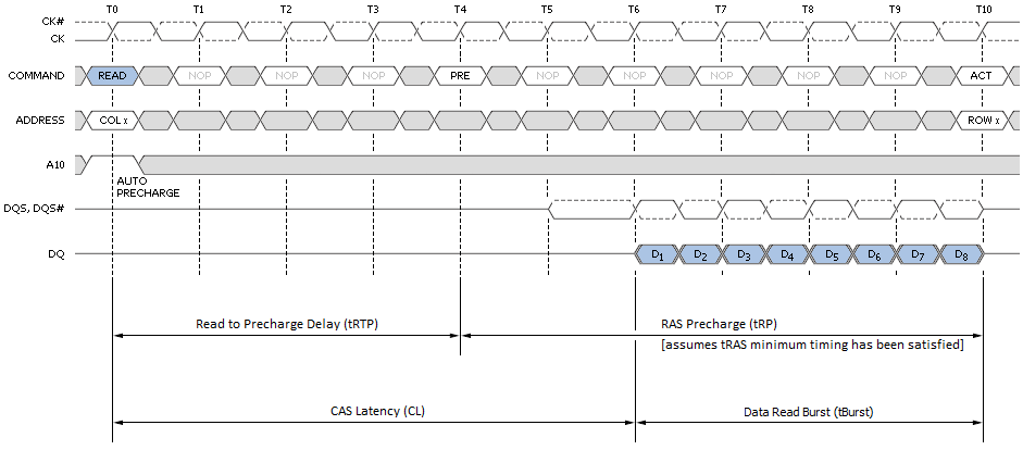
Figure 6 shows the minimum read latency associated with a best-case page-hit scenario. For a part with a CAS Latency of 6T, the memory controller waits only six short clocks before the start of data return. During a Read with Auto-Precharge, the Read command will execute as normal except the active bank will begin precharging CAS-latency (CL) clock cycles before the end of the burst. This feature allows the precharge operation to be partially or completely hidden during periods of burst read cycles, dependent on CL. When tuning our systems we always seek to set tRTP such that tRTP + tRP equals CL + tBurst for exactly this reason. Put another way, if CL and tRP are the same set 4T for DDR3 (2T for DD2).
Sequential reads to the same page make these types of transactions even more profitable as each successive access can be scheduled at a minimum of tBurst (4T) clocks from the last. The timing is captured as the CAS-to-CAS Delay (tCCD) and is commonly referred to as 'Back-to-Back CAS Delay' (B2B), as shown per Figure 7. This feature makes possible extremely high data transfer rates for total burst lengths of one page or less - in our case, 8KB.

Click to enlarge
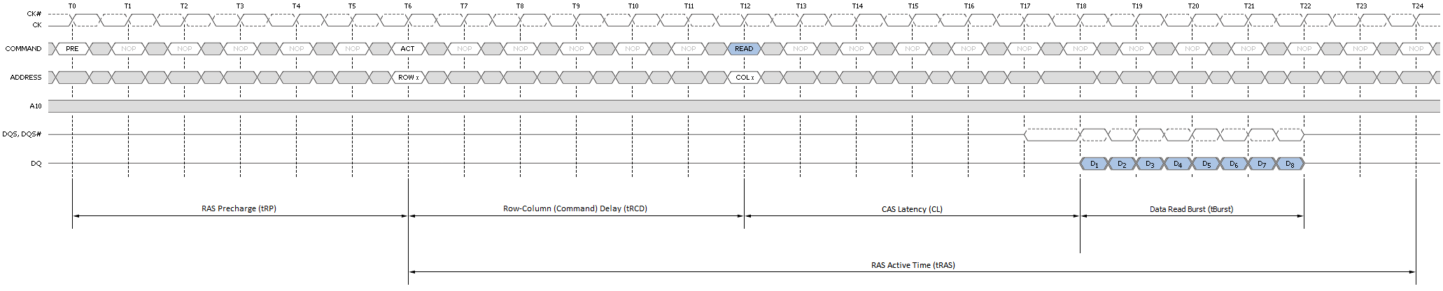
Although not ideal, a page-empty access is still preferred to a miss. In this case the bank to be accessed is Idle with no page open. Common sense tells us any attempt to read or write data to a page in this bank first requires we Activate the bank. In other words, nominal access latency now includes the time to open the page - Row-Column (or Command) Delay (tRCD). This is a doubling of the minimum access latency when compared to that of the page-hit case! Twelve cycles (tRCD + CL) now elapse before the first word is returned. Figure 8 shows this the detail.
![]()
Click to enlarge
Finally, as if the relative penalty of page-empty access wasn't bad enough, here comes page-miss. A miss occurs anytime a memory transaction must first close an open page in order to open an alternate page in the same bank. Only then can the specified data access take place. First closing an open page requires a Precharge, adding the RAS Precharge (tRP) delay to any already lengthy operation. As you can see by Figure 9, the nominal latency of an access of this type is three times that of one page-hit operation!
Click to enlarge
The relative gain/loss ratio for each access type can be quickly assessed simply through a cursory review of the most basic device timings. Imagine a memory kit rated for operation at DDR3-1600, 6-6-6-18 (CL-tRCD-tRP-tRAS): With nothing more we can estimate six cycles for a page-hit access, 12 cycles for a page-empty access, and 18 cycles for a page-miss access.
Normalized to the page-hit access latency, page-empty access is twice as long, and page-miss access is a whole three times as long. If we combine this with what we know about the inner functions of the SDRAM state machine we see page-hit and page-miss are really just subsets of the same bank state (active). Of course, page-empty access necessarily implies an idle bank. The following proof rewards us with some powerful insight.
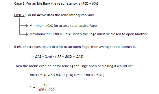
The variable n also represents the percentage of accesses to banks with open pages that must result in a page-hit access if we are to simply pace the nominal access latency that would be achieved if every read access was to an idle bank. And the only thing this depends on is the RAS Precharge delay and the Row-Column (or Command) Delay of the device in question.
You would think by working to maximize n, performance would be maximized as well. And you'd be right. Let's take what we've learned thus far and step it up a notch. We promise, after this you'll never see memory timings in the same light ever again.
Before proceeding, we've prepared a video for those of you that would like to view a few simple animations meant to help visualize each transaction type:


46 Comments
View All Comments
bowhe - Tuesday, October 26, 2010 - link
Thanks for these great articles!What I didn't understand yet:
You state "Installing more than one DIMM per channel does not double the Memory Bus bandwidth, as modules co-located in the same channel must compete for access to a shared 64-bit sub-bus; however, adding more modules does have the added benefit of doubling the number of pages that may be open concurrently (twice the ranks for twice the fun!)". This sounds very positive, but:
Some system manufacturers state that with 3 dimms the memory frequency can be for example 1333MHz, but with 6 dimms it needs to drop to 800MHz. Why does the frequency need to drop when using 6 versus 3 dimms? Does this apply to high end boards like the Gigabyte-X58A-UD9?
Some manufacturer states in a small side note of a 24GB kit (6x4GB) that the stated frequency/timing is only guaranteed when using 3 dimm slots. This leads me to think that any 3 dimms of the set can do the stated timing, but when all are used something inherent in the design or interaction of the i7 processor, motherboard and dimm prevents the use of stated frequency/timings? What is it?
Can one overcome these limitations by adjusting voltages in a high end board like the Gigabyte-X58A-UD9? (without use of extreme cooling <32F/0C)
Thanks a lot!
kakfjak - Thursday, May 5, 2011 - link
www.stylishdudes.com
All kinds of shoes + tide bag
Free transport
cochleoid - Tuesday, March 12, 2013 - link
"When associated in groups of two (DDR), four (DDR2) or eight (DDR3), these banks form the next higher logical unit, known as a rank. "This mislead me. DDR2 may have coincidentally introduced 3 bit banks - allowing for 8 bank chips - but a typical old SDRAM (no DDR) chip had 4 banks.
"We can now see why the DDR3 core has a 8n-prefetch (where n refers to the number of banks per rank) as every read access to the memory requires a minimum of 64 bits (8 bytes) of data to be transferred. This is because each bank, of which there are eight for DDR3, fetches no less than 8 bits (1 byte) of data per read request - the equivalent of one column's worth of data. Whether or not the system actually makes use of all 8 bytes of transferred data is irrelevant. Any delivered data not actually requested can be safely disregarded as it's just a copy of what is still retained in memory."
This threw me off even more. What's happening is that the data at 8 consecutive (or otherwise close, depending on the burst mode) column addresses is being bursted on each read. "n" refers to the width of the memory chip, or the size of the "word" at a particular column address. "n" does not have any relation to the number of banks in a rank.
8 8bit-wide DDR3 chips would make a total module width of 64 bits or 8 bytes at each column address. 8 column addresses would be 64 bytes (not 8 bytes, as the article seems to suggest), which actually corresponds to the cacheline size on most PCs.
SDRAM could burst in sizes of 1,2,4,8
DDR could burst in sizes of only 2,4,8
DDR2 could burst in sizes of only 4,8
DDR3 can burst only in 8.
(All of these could burst in 8, filling the 64 byte cachline in one read operation. The difference with the generations of DDR has been a larger minimum wait in interface clock cycles as the interface got faster and the row accesses remained sluggish.)
The internal clock of SDRAM has been limited by the speed of row accesses. What the 2n,4n,8n prefetches are doing is transferring more of this data available in an open row out at higher interface speeds with the rest of the system. It has nothing to do with the banks.
SDRAM chips were segmented into independently operating banks so that parallel operations on interleaved banks could be synchronized or pipelined. 2n, 4n, and 8n prefetch buffering can be applied without independently operating banks.
ricardo_sa - Saturday, March 26, 2016 - link
Thanks for the detailed explanation. You really saved my day. Ive read this article some time ago to help me understand how a DDR3 worked (theres few detailed explanations on google) and it turned out to be the worst mistake possible. I got the concepts wrong because of the incompetence of the publisher and lost a lot of time dealing with that 8 Bank misconception about the 64 bits.So it turns out one can only write a burst at 1 bank at a time, am i right? Otherwise you could access all the 8 banks in one single write/read....
Huendli - Friday, March 13, 2015 - link
Thanks for this interesting read with much attention to detail!"a top priority [...] should be to focus development on reducing absolute minimum latency requirements for timings such as CAS and tRCD, rather than chasing raw synthetic bandwidth figures or setting outright frequency records at the expense of unduly high random access times."
The latter's exactly what happened. DDR3-1600 modules with CL7 timings were widely available at the time this article had been written. Nowadays, you only get ridiculously-named bars with equally-ridiculously monstrous heatspreaders, but more bandwidth and worse timings than ever.
Anuradha - Tuesday, March 9, 2021 - link
Each rank consists of 8 banks, OR, each rank consists of 8 ICs and each IC consists of 8 banks??