NVIDIA’s GeForce GTX 460: The $200 King
by Ryan Smith on July 11, 2010 11:54 PM EST- Posted in
- GPUs
- GeForce GTX 400
- GeForce GTX 460
- NVIDIA
GF104: NVIDIA Goes Superscalar
When the complete GF100 GPU was presented to us back at CES 2010 in January, NVIDIA laid out a design that in turn had a very obvious roadmap to go with it. With GF100’s modular design, derivatives of the card would be as simple as fabricating GPUs with fewer GPCs and ROPs (at least until you got to the sub-$100 market). This is the route we expected NVIDIA to take with GF104, removing 1 or 2 GPCs to make a smaller chip.
What they threw us instead was a curveball we were not expecting.
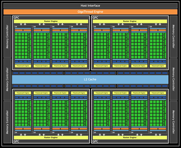
Let’s start at a high level. On GF100, there were 4 GPCs each containing a Raster Engine and 4 SMs. In turn each SM contained 32 CUDA cores, 16 load/store units, 4 special function units, 4 texture units, 2 warp schedulers with 1 dispatch unit each, 1 Polymorph unit (containing NVIDIA’s tessellator) and then the L1 cache, registers, and other glue that brought an SM together.
NVIDIA GF100 - Full Implementation, No Disabled Logic
GF104 in turn contains 2 GPCs, which are effectively the same as a GF100 GPC. Each GPC contains 4 SMs and a Raster Engine. However when we get to GF104’s SMs, we find something that has all the same parts as a GF100 SM, but in much different numbers.
NVIDIA GF104 - Full Implementation, No Disabled Logic
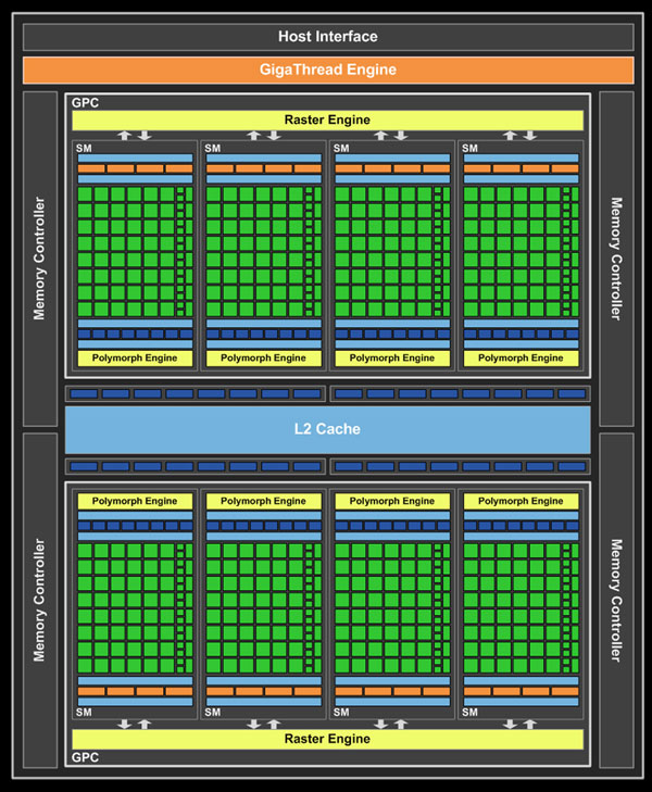
The biggest and most visible change is that NVIDIA beefed up the number of various execution units per SM. The 32 CUDA cores from GF100 are now 48 CUDA cores, while the number of SFUs went from 4 to 8 along with the texture units. As a result, per SM GF104 has more compute and more texturing power than a GF100 SM. This is how a “full” GF104 GPU has 384 CUDA cores even though it only has half the number of SMs as GF100.
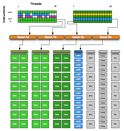
One thing we haven’t discussed up until now is how an SM is internally divided up for the purposes of executing instructions. Since the introduction of G80 in 2006, the size of a warp has stayed constant at 32 threads wide. For Fermi, a warp is executed over 2 (or more) clocks of the CUDA cores – 16 threads are processed and then the other 16 threads in that warp are processed. For full SM utilization, all threads must be running the same instruction at the same time. For these reasons a SM is internally divided up in to a number of execution units that a single dispatch unit can dispatch work to:
- 16 CUDA cores (#1)
- 16 CUDA cores (#2)
- 16 Load/Store Units
- 16 Interpolation SFUs (not on NVIDIA's diagrams)
- 4 Special Function SFUs
- 4 Texture Units
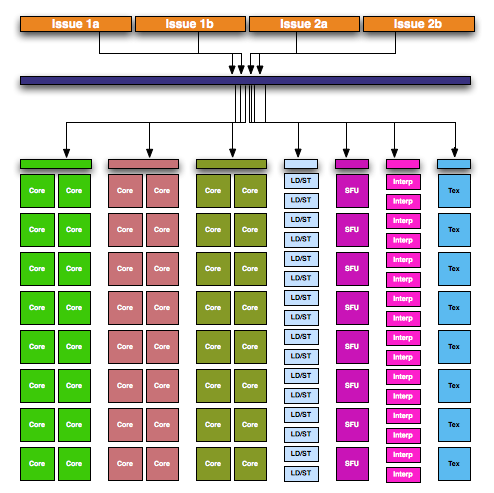
With 2 warp scheduler/dispatch unit pairs in each SM, GF100 can utilize at most 2 of 6 execution units at any given time. It’s also because of the SM being divided up like this that it was possible for NVIDIA to add to it. GF104 in comparison has the following:
- 16 CUDA cores (#1)
- 16 CUDA cores (#2)
- 16 CUDA cores (#3)
- 16 Load/Store Units
- 16 Interpolation SFUs (not on NVIDIA's diagrams)
- 8 Special Function SFUs
- 8 Texture Units
This gives GF104 a total of 7 execution units, the core of which are the 3 blocks of 16 CUDA cores.
GF104 Execution Units
With 2 warp schedulers, GF100 could put all 32 CUDA cores to use if it had 2 warps where both required the use of CUDA cores. With GF104 this gets more complex since there are now 3 blocks of CUDA cores but still only 2 warp schedulers. So how does NVIDIA feed 3 blocks of CUDA cores with only 2 warp schedulers? They go superscalar.
In a nutshell, superscalar execution is a method of extracting Instruction Level Parallelism from a thread. If the next instruction in a thread is not dependent on the previous instruction, it can be issued to an execution unit for completion at the same time as the instruction preceding it. There are several ways to extract ILP from a workload, with superscalar operation being something that modern CPUs have used as far back as the original Pentium to improve performance. For NVIDIA however this is new – they were previously unable to use ILP and instead focused on Thread Level Parallelism (TLP) to ensure that there were enough warps to keep a GPU occupied.
NVIDIA GF100 SM
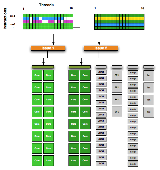
In order to facilitate superscalar operation, NVIDIA made some changes to both the warp scheduler and the dispatch unit for GF104. Each warp scheduler is now connected to 2 dispatch units, giving it the ability to dual-issue instructions. Along with its regular duties, a warp scheduler is now responsible for organizing its superscalar operation by analyzing the next instruction in its warp to determine if that instruction is ILP-safe, and whether there is an execution unit available to handle it. The result is that NVIDIA’s SMs now handle superscalar operation similar to that of a CPU, with the hardware taking the responsibility for dispatching parallel instructions. This in turn means that GF104 can execute a warp in a superscalar fashion for any code and including old CUDA code, allowing it to extract ILP out of old and new code alike. The GF104 compiler in NVIDIA’s drivers will try to organize code to better match GF104’s superscalar abilities, but it’s not critical to the ability.
NVIDIA GF104 SM - Note, more instructions in flight per SM vs. GF100
Ultimately superscalar execution serves 2 purposes on GF104: to allow it to issue instructions to the 3rd CUDA core block with only 2 warps in flight, and to improve overall efficiency. In a best-case scenario GF104 can utilize 4 of 7 execution units, while GF100 could only utilize 2 of 6 execution units.
The upside to this is that on average GF104 should be more efficient per clock than GF100, which is quite a remarkable feat. The downside to this is that now NVIDIA has a greater degree of best and worst case scenarios, as requiring superscalar execution to utilize the 3rd CUDA core block means that it’s harder to use that 3rd block than the previous 2. The ability to extract ILP from a warp will result in GF104’s compute abilities performing like a 384 CUDA core part some of the time, and like a 256 CUDA core part at other times. It will be less consistent, but on average faster than a pure 256 CUDA core part would be.
With the addition of superscalar abilities, GF104 marks the slow-but-steady merger of the CPU and the GPU. GF104 is now just a bit more CPU-like than GF100 was, a particularly interesting turn of events since we’re looking at a waterfall part and not a new architecture today.


93 Comments
View All Comments
GeorgeH - Monday, July 12, 2010 - link
I actually think it should be called a 460. People with a reasonable amount of tech knowledge are going to know the difference, and people without it are already trained to think that a bigger RAM number is always better (see the tons of "bargain" cards with 1GB+ of slow DDR.)Basically, the performance differential here is already clear from the full product name, and we have one fewer model number muddying a GPU market already overflowing with a ridiculous amount of model names that have identical, nearly identical, or completely misleading performance capabilities relative to other model names.
Daeros - Monday, July 12, 2010 - link
I would agree with you except for the common practice of mfg's doubling up on VRAM. When that happens, there will be 768MB, 1GB, 1.5GB, and 2GB versions, and people will have no idea the 1.5GB will probably be slower than the 1GB version.tigersty1e - Monday, July 12, 2010 - link
This line made me read it twice."This in turn means the blades of the fan sit at the same height as the lip, blocking direct airflow out the back. With this design the card is still exhausting at least some air out of the rear of the card, but it shouldn’t be as much as a fully-open card such as our custom Asus GTX 460."
rear and back are the same thing. I think you meant to say the the cover blocks direct airflow out the front.
Ryan Smith - Monday, July 12, 2010 - link
I define the front of the card to be the side with the display ports, so the cover blocks airflow out of the opposite end, the back.fausto412 - Monday, July 12, 2010 - link
While a very nice card...too little too late...i got a 5870 3 weeks ago. if you have a high end quad core and want to play BFBC2 in the highest settings only a gtx480 or 5870 will do. i chose the cheaper, cooler and more efficient card.kumquatsrus - Monday, July 12, 2010 - link
or gtx 460 in sli for less?Jamahl - Monday, July 12, 2010 - link
Yeah look around, not just at Anand's flawed benches.TPU shows sli 460's losing to the 5970 by 20% at 1680 and 1920, and a massive 30% at 2560.
They aren't even close, but keep dreaming anyway.
DominionSeraph - Tuesday, July 13, 2010 - link
The reply was to a 5870, not 5970. Just a matter of $300 difference between the two.DrMrLordX - Monday, July 12, 2010 - link
On your power consumption + noise charts (at the very least), the Zotac card's results are shown with white text superimposed over a yellow bar on the graph. This makes the white text almost completely unreadable. One can guess at the numbers based on context, but still . . .bobjones32 - Monday, July 12, 2010 - link
The benchmarks look good at first look, but then I realized I purchased my current 4870 for $150 nearly a year and a half ago.Looking more closely at these benchmarks, the GTX 460 beats the 4870 in most tests, but not by that much, and at lower resolutions the 4870 actually wins.
Shouldn't it be clear-cut that a $200 brand new card from today destroys a $150 card from nearly a year and a half ago?