EVGA P55 FTW - It's Here...Pictorial Preview
by Rajinder Gill on August 10, 2009 11:07 PM EST- Posted in
- Raja's Ramblings
Sorry folks, we actually have another shameless P55 motherboard picture preview for you. I know Gary thought his ASRock article was the last of them, but EVGA released us this evening to discuss their flagship P55 (E657) FTW (For The Win) product. We know you are urging us to break rank at this point and post up some heavy overclocking benchmarks and performance comparisons against the i7 platform, but there is little chance of getting away with anything other than a few pictures to look over until the platform embargo lifts.
We are not quite sure at this point of how many users will be attracted to higher cost i5 boards given the fact that that total platform cost overlaps the cost of entry-mid level i7 offerings. However, this has not deterred any of the big players from putting together a top-end i5 package based upon a combination of features they think will reel in customers. Early pricing lists of i5 boards are putting the top-end offerings between the $200~$250 mark, this one is no different with an estimated MSRP of $250 (there will be a few sub $200 models offered as well as an NF200 'Classified' variant of the board we're previewing today).
Any board following in the footsteps of the EVGA X58 Classified has a lot to live up to. Early overclocking tests on the i5 platform have revealed a similar trend to what we saw on the X58/i7 motherboards when used with sub-zero cooling, with the top-end EVGA P55 boards ahead of the competition by the slimmest of margins as we move into the final tweaking stage before full retail release.
It is not a massive gap at this point, we are talking a 3-5 BCLK difference between this board and the ‘best of the rest’ given the same hardware configuration and voltages. For the more conventional user (those using air and water cooling), our take is that you won’t find any overclocking advantage comparing one enthusiast board over another, assuming functionality is completely up to speed.
There are a number of unique hardware features that EVGA hopes will help keep their top line boards ahead of the pack when really pushed by an enthusiast. EVGA has gone the extra mile by providing onboard hardware components that make fine adjustment compensation for all major signal lines possible among other items. Team these functions with sub-zero boot-up & current limit manipulation jumpers and we begin to see that EVGA is making a full assault for the P55 overclocking crown.
Companies such as EVGA, DFI and MSI continue with a purist approach to PWM design for all major power rails. We happen to sit with the camp that believes in the importance of fast transient response and low noise attributes first. The proof is in the pudding and we’re eager to compare several boards side by side to see if any additional overclocking headroom can be realized that supports the ‘more phases=unconditionally better’ theory.
Initial in lab tests indicates that the only thing that really matters from a user perspective is that the given PWM design is capable of pumping out the required current comfortably and cleanly. The rest comes down to heat management and ease of cooling; anything more seems to be a matter of marketing rather than real substance.
Other than costs, we cannot see a reason why it is not possible to keep a reasonable phase count by using suitably sized MOSFET’s with a decent heat sink and capable buck controller. We think it would be of more use to all concerned if companies would simply inform all of us how much current their PWM circuits can supply rather than tell us about XXX number of phases, which on its own does not tell us anything at all.
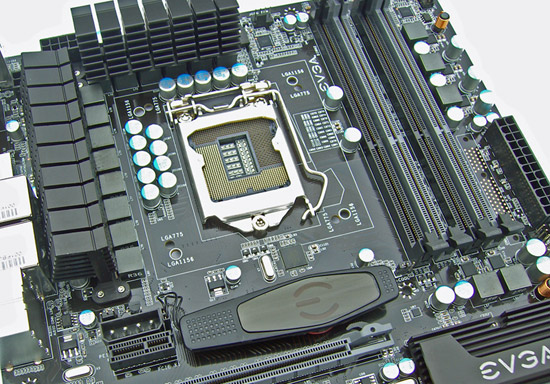
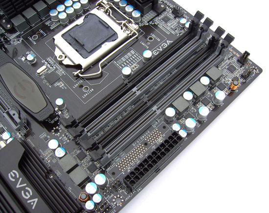
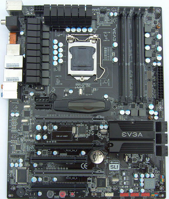
In the case of the E657 FTW, CPU power is supplied by a 600W peak current capable 12-phase supply (more than i5 will ever need). VTT and memory power is supplied by 2 and 3 phase supplies respectively, both using the same model of FET’s as used for the CPU. You’ll also notice that EVGA has added socket 775 mounting holes at a slight angle from the 1156 holes, a welcome addition for those of you with a good 775 heat sink or those of you concerned about needing new socket mounts for those trusted LN2 pots and phase change coolers.
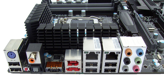
The rear panel contains 6 USB ports, PS2 keyboard port, 2 ESATA ports, 1x1394a port, dual Marvell Gigabit LAN ports and the audio panel driven by the popular Realtek ALC889 HD codec. A CMOS clear button is provided on the rear panel for ease of use when the board is mounted in a case.
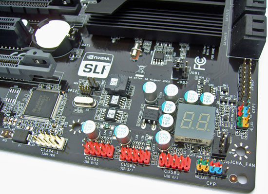
A Hex postcode display is available for debugging purposes together with an output connecter for EVGA’s OCP (overclocking panel) which helps users work around the somewhat quirky boot-up voltage requirements of sub-zero cooled processors. An additional 6 USB ports are supported via internal headers, plus an extra 1394a header.
Three onboard BIOS chips are present allowing users to store different BIOS revisions for testing purposes or as a failsafe backup. BIOS chip selection is made possible by a simple three-position slider switch placed at the lower left corner of the board.
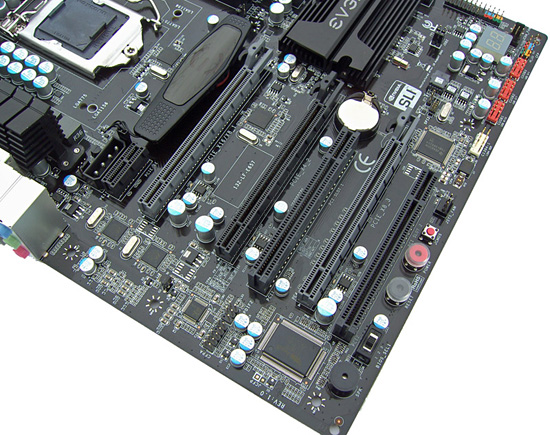
Looking over the slot layout; we have one PCIe 2.0 x1 slot, two PCI slots, and three PCIe 2.0 x16 slots providing x16/x4 or x8/x8/x4 lane allocation (depending upon usage). Seven (1 CPU + 6 additional) fully controllable fan headers are placed in various locations, five of which are easily accessible at all times regardless of component loading.
Onboard power, reset and CMOS clear buttons are placed at the lower edge of the board for those of us that like to test and use boards on an open testbed (the reset button doubles up as a flashing LED to show SATA activity).
That about rounds up today's quick preview, the official release is not far off so please bear with us...


54 Comments
View All Comments
flipmode - Tuesday, August 11, 2009 - link
The fact that you can put a 775 heatsink on here is worth some real money to those with some nice $30-$60 775 heatsinks.Um, what the HECK is the "purist approach" to power phase design? Is it "more is better" or "quality is better"? Just trying to be "in the know".
Rajinder Gill - Tuesday, August 11, 2009 - link
Purist in the sense of a design not relying on external multiplexers to sub-divide phases for a pseudo phase effect. In most cases the current is still limited by the buck controller no matter how you sub-divide downstream. Point is, you can have 24 phases supplying 300~400w peak or a 12 phase solution supplying 600w. SO when motherboard vendors advertise their boards under the guise of phase count - its really not telling us much at all. There really is no need for a multitude of phases adding extra complexity to the design plus additional switching noise when you can make a fast transient response supply by using the right parts and a less complex topology.MadMan007 - Tuesday, August 11, 2009 - link
Multiphase designs can be cheaper to implement if they use more cheap parts rather than fewer expensive ones. Given the way mobo manufacturers penny pinch I am certain that's the real reason lots of phases have become fashionable, it also helps that it's easy to market 'MOAR=BETTAR' to the enthusiast crowd which isn't aware of the real details of power supply design.anandreader - Tuesday, August 11, 2009 - link
Good to see the 3 bios backups - presumably, the two offline chips aren't writable unless the slider switch is set to them?What I think would be the best rootkit defense is a method to overwrite the functioning bios at post time by pressing a button. That would restore the bios to a known good state. If you want to flash a new bios from the OS, you still have to push the button or flip a toggle before the chip is writable. Once the bios write button was pressed, the flash utility could proceed. So pressing the button at post time says - "overwrite the current bios". Pressing the same button at os time says - "yeah, it's ok to flash a new bios but if I press this button at post time, erase what I'm about to write."
That way, a rootkit wouldn't be able to stealth its way into the bios. And if it somehow did, the post-time button press would wipe it with the factory bios. That means the factory bios would have to be in some sort of ROM.
Furuno - Tuesday, August 11, 2009 - link
Hey, there's some solder pads beside the memory slots. I wonder what's that for?strikeback03 - Tuesday, August 11, 2009 - link
Read the silkscreen - Braidwood.Casper42 - Tuesday, August 11, 2009 - link
Wonder why they didnt include the connector?For an OC Board, I would think they would want to give you the option of Braidwood assist for conventional Hard Drives.
Nickel020 - Tuesday, August 11, 2009 - link
I noticed that the board has two EPS12V connectors, are these actually required or does it work when you only connect one?If it actually requires the two then it's quite strange that EVGA decides to release such a board. The vast majority of potential customers will not have a PSU like that, and people who have one are likely already using a Nehalem. That leaves EVGA with hardcore overclockers that want to achieve WR on P55, but it's an economically questionable decision to release a board jsut targeted at that crowd.
The board does look quite good though, the only "problem" I see is the placement of the CF/SLI molex 4-pin.
mindless1 - Thursday, August 20, 2009 - link
If you were to very extreme overclock, THEN you would need both to supply the current the PWM subcircuit can handle since the wires and connector contacts have inherent limits in current. Otherwise, for normal overclocking you could use only one connector.AznBoi36 - Wednesday, August 12, 2009 - link
I've got 2x EPS12V connectors on my Corsair HX1000 :)But I'm already on i7 so no need for P55 :)