The RV870 Story: AMD Showing up to the Fight
by Anand Lal Shimpi on February 14, 2010 12:00 AM EST- Posted in
- GPUs
What Made it All Ok: 4 GPUs in < 6 Months
Through a lot of hard work and sacrifice, even on Carrell’s part, ATI cut the RV870 from as much as 22mm on a side down to roughly 18mm x 18mm. The problem is that RV770 was around 16mm on a side. The RV870 was still too big.
Carrell wanted to cut it down even more, but two things changed his mind. First, in order to build 870 in the space of a 770 ATI would have to cut out much more from the chip than Carrell originally tought. One of the things that would have to go was some of the shader core.
In order to run the GDDR5 memory at the sort of data rates that ATI was targeting for the 5870 the analog PHYs on the chip had to grow considerably. At 16mm on a side ATI would either have to scale back memory bandwidth or eat into the shader core area. Either way we would’ve had a slower chip.
I asked Carrell if 16mm on a side would’ve made the RV870 $100 cheaper at launch, putting it on par with the RV770 launch prices. He said no. I didn’t find out why until much later, but I’ll save that story for another time.
Sacrificing performance to meet the 16mm x 16mm die size targets wasn’t going to happen, but what ultimately convinced Carrell to go with a larger die this time around was something that ATI didn’t get nearly enough praise for: the ability to launch 4 different 40nm DirectX 11 GPUs in less than 6 months.
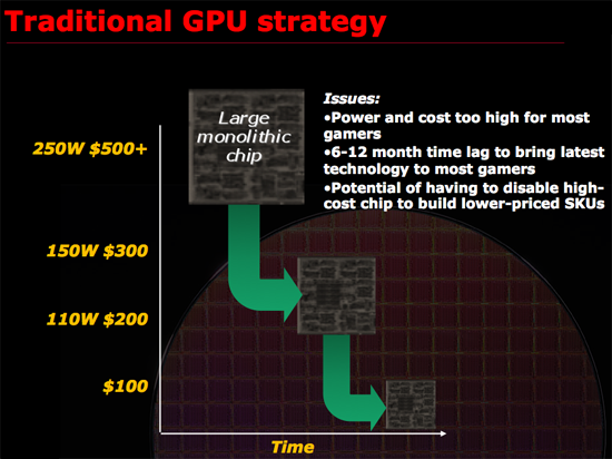
Remember that Carrell’s beef with building the biggest GPU possible is that it takes too long for the majority of customers to get access to derivatives of that GPU. Look at how long it took G80 or GT200 to scale down. And who knows when we’ll see $150 Fermi/GF100 derivatives.
But ATI Engineering promised two things. First, that Cypress would have a successor called Juniper that would be ready around the same time. Secondly, two more GPUs would follow and the whole stack will be done and out in less than 6 months. ATI came close in 2008 with 3 GPUs in 3 months, but the fourth member of the 4000 series didn’t show up until April of 2009.
It wasn’t an impossible feat. ATI does have concurrent design teams and a lot of engineering resources in India/China. By working on Juniper in tandem with Cypress, assuming there were no show stopping bugs, ATI could exploit efficiencies in two teams effectively working on the same hardware (Juniper was just half a Cypress).
The idea of taking such a huge risk made Carrell uncomfortable. Running two GPU designs in parallel, for the same family of chips, is risky. If everything works out perfectly, you get two chips out at the same time. If it doesn’t, you’ve just tied up two design teams on one product generation. A slip here would give ATI its own Fermi.
What ultimately sold Carrell was the fact that engineering told him that they believed they could pull it off. Carrell believes in people. He believes if you expect the best out of those around you, then that’s what you’ll get. He couldn’t reconcile his beliefs with doubting the schedule engineering was feeding him. Carrell nervously signed off and the Evergreen stack was born.
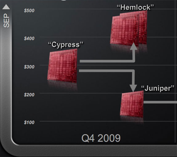
Cypress and Juniper were delivered nearly at the same time. In fact, Juniper was ready a bit earlier and was sampled to developers months before ATI launched the 5000 series. Cedar and Redwood followed, not to mention a dual-Cypress board that became the Radeon HD 5970. And all of this was done and ready in less than 6 months (the chips themselves were all ready within 4 months).
When the smoke cleared ATI had new DirectX 11 parts at $600, $400, $300, $200, $150, $100 and $60. The Windows 7/DirectX 11 market bulge just got serviced.


132 Comments
View All Comments
Dudler - Sunday, February 14, 2010 - link
Whoa... Just Whoa.Very insightful and interesting.
Amd moving to GF next generation and Norther Islands this year?
Whoa.
Thx Anand :)
carlhenry - Sunday, February 14, 2010 - link
i really loved the eyefinity being so 'mission impossible'. awesome article!Patrick Wolf - Sunday, February 14, 2010 - link
The first rule of SunSpot: You don't talk about SunSpot. :Dmubeen - Tuesday, February 16, 2010 - link
Such an informative article Mr. Anand. Really appreciate your efforts.just4U - Tuesday, February 16, 2010 - link
I agree it's a great article, nice to see these ones pop up from time to time. It don't really matter to me if it's nvidia, amd or intel.. just having a more insightful read is refreshing.DearSX - Sunday, February 14, 2010 - link
I really do a like article like this. I wonder how old others are cause I'm 25 and I did not even notice how much reading things like this mattered. Its more important than buying something or performance figures imo.Paulman - Sunday, February 14, 2010 - link
I, too, will second that. Really cool. :PMrSpadge - Sunday, February 14, 2010 - link
Many thanks for this interesting article and especially the in-dpeth information about TSMC, the process and how ATI deals with it. Thanks to you, Anand, for writing it and thanks to the good guys at AMD for sharing this information!Beyond excellence :)
hyvonen - Monday, February 15, 2010 - link
And NVidia's call for "zero defects, zero variability" was jaw-dropping. Do they have any idea how silicon is manufactured?Unbelievable cluelessness... with this attitude, they are out of business in the next two years. They are completely unprepared to harness the potential in the latest process nodes.
Meanwhile, it also sounds like TSMC is way over its head in this - uncharacteristic screw-ups with the chamber matching, bad leakage etc. Not to mention the choice to delay HKMG until 28nm (and having to kill 32nm because of that). GF is going to eat them for lunch, and take over the foundry business.
ET - Sunday, February 14, 2010 - link
Indeed. One of the more interesting articles I've read in a while.