The RV870 Story: AMD Showing up to the Fight
by Anand Lal Shimpi on February 14, 2010 12:00 AM EST- Posted in
- GPUs
The Cost of Jumping to 40nm
This part of the story could almost stand on its own, but it directly impacts much of what happened with Cypress and the entire Evergreen stack that it’s worth talking about here.
By now you’ve most likely heard about issues with TSMC’s 40nm process. While the word is that the issues are finally over, poor yields and a slower than expected ramp lead to Cypress shortages last year and contributed to NVIDIA’s Fermi/GF100 delay. For the next couple of pages I want to talk about the move to 40nm and why it’s been so difficult.
The biggest issue with being a fabless semiconductor is that you have one more vendor to deal with when you’re trying to get out a new product. On top of dealing with memory companies, component manufacturers and folks who have IP you need, you also have to deal with a third party that’s going to actually make your chip. To make matters worse, every year or so, your foundry partner comes to you with a brand new process to use.
The pitch always goes the same way. This new process is usually a lot smaller, can run faster and uses less power. As with any company whose job it is to sell something, your foundry partner wants you to buy its latest and greatest as soon as possible. And as is usually the case in the PC industry, they want you to buy it before it's actually ready.
But have no fear. What normally happens is your foundry company will come to you with a list of design rules and hints. If you follow all of the guidelines, the foundry will guarantee that they can produce your chip and that it will work. In other words, do what we tell you to do, and your chip will yield.
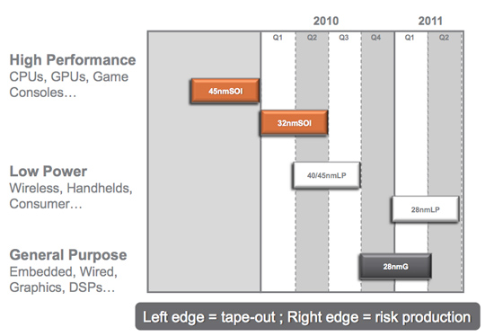
Global Foundries' 2010 - 2011 Manufacturing Roadmap
The problem is that if you follow every last one of these design rules and hints your chip won’t be any faster than it was on the older manufacturing process. Your yield will be about the same but your cost will be higher since you’ll bloat your design taking into account these “hints”.
Generally between process nodes the size of the wafer doesn’t change. We were at 200mm wafers for a while and now modern fabs use 300mm wafers. The transistor size does shrink however, so in theory you could fit more die on a wafer with each process shrink.
The problem is with any new process, the cost per wafer goes up. It’s a new process, most likely more complex, and thus the wafer cost is higher. If the wafer costs are 50% higher, then you need to fit at least 50% more die on each wafer in order to break even with your costs on the old process. In reality you actually need to fit more than 50% die per wafer on the new process because yields usually suck at the start. But if you follow the foundry’s guidelines to guarantee yield, you won’t even be close to breaking even.
The end result is you get zero benefit from moving to the new process. That’s not an option for anyone looking to actually use Moore’s Law to their advantage. Definitely not for a GPU company.
The solution is to have some very smart people in your company that can take these design rules and hints the foundry provides, and figure out which ones can be ignored, and ways to work around the others. This is an area where ATI and NVIDIA differ greatly.


132 Comments
View All Comments
simtex - Sunday, February 21, 2010 - link
Excellent article ;) Insider info is always interesting, makes me a little more happy about my -50% AMD stocks, hopefully they will one go up again.NKnight - Wednesday, February 17, 2010 - link
Great read.- Friday, February 19, 2010 - link
you should write a (few)book(s); of course in multi eReader formats
asH
- Saturday, February 20, 2010 - link
Nvidia blames sales shortfall on TSMChttp://www.eetimes.com/news/latest/showArticle.jht...">http://www.eetimes.com/news/latest/show...E1GHPSKH...
one dot you didnt connect in the article was AMD's foundry experience, which gives AMD a big advantage over NVIDIA; must have been an oversight?
asH
truk007 - Tuesday, February 16, 2010 - link
These articles are why I keep coming here. The other sites could learn a lesson here.dstigue1 - Tuesday, February 16, 2010 - link
I think the title says it all. But to add I also like the technical level. You can understand it with some cursory knowledge in graphics technology. Wonderfully written.sotoa - Tuesday, February 16, 2010 - link
Excellent work and very insightful indeed!juzz86 - Tuesday, February 16, 2010 - link
An amazing read Anand, I can wholeheartedly understand why you'd enjoy your dinners so much. One reader said that these were among the best articles on the site, and I have to agree. Inside looks into developments in the industry like this one are the real hidden gems of reviewing and analysis today. You should be very proud. Thanks again. Justin.talon262 - Tuesday, February 16, 2010 - link
Hell of an article...congrats to Anand for putting it out there and to the team at ATI for executing on some hard-learned lessons. Since I have a 4850 X2, I'm most likely going to sit Evergreen out (the only current ATI card that specs higher than my 4850 X2 (other than the 4970 X2) is Hemlock/5970 and Cypress/5870 would be a lateral move, more or less); while I run Win7, DX11 compatibilty is not a huge priority for me right this moment, but I will use the mid-range Evergreen parts for any systems I'll build/refurb over the next few months.Northern Islands, that has got me salivating...
(Crossposted at Rage3D)
Peroxyde - Monday, February 15, 2010 - link
Thanks for the great article. Do you have any info regarding ATI's commitment to the Linux platform? I used to see in Linux forums about graphics driver issues that ATI is the brand to avoid. Is it still the case?