P55 Overclocking Showdown - ASUS, Gigabyte, and EVGA at the OC Corral (Page 6 Updated)
by Rajinder Gill on November 6, 2009 12:00 PM EST- Posted in
- Motherboards
RTL -
A quick note for all you benching fanatics on the 1156/1366 platform, especially those of you that love Super Pi. ‘Round Trip Latency’ chipset function in BIOS denotes the number of Uncore Clock cycles that pass before data arrives back at the IMC after a read command is issued.
For those of you familiar with socket 775 and the P35/P45/X38/X48 chipsets, this setting is known as tRD, aka ‘Performance Level’.
‘Performance Level’ on socket 775 based processor architectures denotes the number of Front Side bus clock cycles that pass before data arrives back from the memory banks time aligned with the leading edge of a FSB clock cycle, making data transfer between the two clock domains possible.
For the i5 and i7 architectures the data read time (from the time the read command was issued) can be calculated by the following formula;
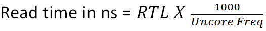
Needless to say, the smaller the figure in nanoseconds, the better the performance. However, there is a change here in that although we are given control of the RTL parameter for each memory channel, the default time calculated by the memory controller at POST is almost as fast as the gearing for clock crossing can go based on aggressive timing values set by Intel.
Manual control of the RTL function has been added by board vendors to P55/X58, primarily to allow looser manual settings or to lock the setting down to a known working value. The latter is required at times because there are instances where the IMC selects a non-ideal/unstable setting for one of the memory channels, in which case locking these values down to a stable setting prevents random crashes and bizarre system instability between system reboots. Changes of 1-2 clocks below the auto-selected RTL value are sometimes possible for light load benchmarks such as a single thread of Super Pi 32M thus giving a small boost in the final time.
Socket 1156 CPU’s have their Uncore frequency multiplier locked, so there’s not too much to look out for other than a quick glance at the real RTL time in nanoseconds, to make sure that the clock crossing schedule is just as fast if not faster than your previous selected overclock.
For those of you playing around with socket 1366 processors, you get some control over the Uncore multiplier ratio (so long as you observe the minimum 2x memory multiplier rule). Bear in mind that as you increase the Uncore frequency, the RTL value will increase because more clock cycles pass over the same time period. As an example, if RTL defaults to a value of 54 clocks at an Uncore frequency of 4GHz (20x Uncore multiplier) and a memory CAS of 8, our effective read turnaround time is;
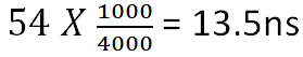
Assuming all other bus frequencies and memory timings are unchanged, if we decide to increase the Uncore Multiplier ratio to 21X, the RTL value should move out to around 57 clocks;
Any greater than 13.57ns, and we have lost system performance and as a double whammy will also have to increase memory controller voltage to facilitate the higher switching speed of the associated IMC stages; this is not the way to truly ‘overclock’ a system for better performance.
The reason we’re including this simple formula here is so that users can simply boot the motherboard, read the RTL value and quickly plug the numbers into the formula to work out the read time. This should help users from running repeated benchmarks for every given change in CAS and tRCD or change of a memory multiplier ratio. As always, various benchmarks will react to Uncore frequency changes in different ways, although it is handy to know if your selected operating point allows for tighter memory controller gearing than other available combinations.
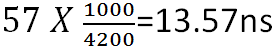
We've been toying around with RTL for a few days and believe we've come up with a method of reliably predicting RTL in clocks using the following formula;
tCL denotes the True CAS Latency of the memory modules, giving us the time required to access memory at a given CAS and memory operating frequency. We take the tCL value, add it to the Uncore period we add ~670ps (approx distance to the DIMM) for each read transfer then multiply this by eight.
Do note, that the 0.67 part of the formula may need slight adjustment according to board layout; If a vendor places the DIMM slots closer to the CPU this figure will need to be reduced. You will also need to reduce this figure to around ~0.57 (570ps) for very high memory clock frequencies on some motherboards. This is because the clock skew needs to be advanced as memory clock frequency is increased. A simple Excel based calc is available if required, send me an email!


52 Comments
View All Comments
SpaceRanger - Friday, November 6, 2009 - link
[quote]Gigabyte’s top end offering comes in at $*** and touts their answer to competing boards as having ’24-Phase’ PWM circuit (using a multiplexed ISL6336 6 phase controller).[/quote]So all it takes is 3 stars to get the top end offering from Gigabyte?
Rajinder Gill - Friday, November 6, 2009 - link
Sorry, that skipped through edit - corrected.