AMD's Radeon HD 5870: Bringing About the Next Generation Of GPUs
by Ryan Smith on September 23, 2009 9:00 AM EST- Posted in
- GPUs
More GDDR5 Technologies: Memory Error Detection & Temperature Compensation
As we previously mentioned, for Cypress AMD’s memory controllers have implemented a greater part of the GDDR5 specification. Beyond gaining the ability to use GDDR5’s power saving abilities, AMD has also been working on implementing features to allow their cards to reach higher memory clock speeds. Chief among these is support for GDDR5’s error detection capabilities.
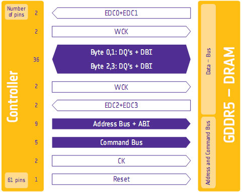
One of the biggest problems in using a high-speed memory device like GDDR5 is that it requires a bus that’s both fast and fairly wide - properties that generally run counter to each other in designing a device bus. A single GDDR5 memory chip on the 5870 needs to connect to a bus that’s 32 bits wide and runs at base speed of 1.2GHz, which requires a bus that can meeting exceedingly precise tolerances. Adding to the challenge is that for a card like the 5870 with a 256-bit total memory bus, eight of these buses will be required, leading to more noise from adjoining buses and less room to work in.
Because of the difficulty in building such a bus, the memory bus has become the weak point for video cards using GDDR5. The GPU’s memory controller can do more and the memory chips themselves can do more, but the bus can’t keep up.
To combat this, GDDR5 memory controllers can perform basic error detection on both reads and writes by implementing a CRC-8 hash function. With this feature enabled, for each 64-bit data burst an 8-bit cyclic redundancy check hash (CRC-8) is transmitted via a set of four dedicated EDC pins. This CRC is then used to check the contents of the data burst, to determine whether any errors were introduced into the data burst during transmission.
The specific CRC function used in GDDR5 can detect 1-bit and 2-bit errors with 100% accuracy, with that accuracy falling with additional erroneous bits. This is due to the fact that the CRC function used can generate collisions, which means that the CRC of an erroneous data burst could match the proper CRC in an unlikely situation. But as the odds decrease for additional errors, the vast majority of errors should be limited to 1-bit and 2-bit errors.
Should an error be found, the GDDR5 controller will request a retransmission of the faulty data burst, and it will keep doing this until the data burst finally goes through correctly. A retransmission request is also used to re-train the GDDR5 link (once again taking advantage of fast link re-training) to correct any potential link problems brought about by changing environmental conditions. Note that this does not involve changing the clock speed of the GDDR5 (i.e. it does not step down in speed); rather it’s merely reinitializing the link. If the errors are due the bus being outright unable to perfectly handle the requested clock speed, errors will continue to happen and be caught. Keep this in mind as it will be important when we get to overclocking.
Finally, we should also note that this error detection scheme is only for detecting bus errors. Errors in the GDDR5 memory modules or errors in the memory controller will not be detected, so it’s still possible to end up with bad data should either of those two devices malfunction. By the same token this is solely a detection scheme, so there are no error correction abilities. The only way to correct a transmission error is to keep trying until the bus gets it right.
Now in spite of the difficulties in building and operating such a high speed bus, error detection is not necessary for its operation. As AMD was quick to point out to us, cards still need to ship defect-free and not produce any errors. Or in other words, the error detection mechanism is a failsafe mechanism rather than a tool specifically to attain higher memory speeds. Memory supplier Qimonda’s own whitepaper on GDDR5 pitches error correction as a necessary precaution due to the increasing amount of code stored in graphics memory, where a failure can lead to a crash rather than just a bad pixel.
In any case, for normal use the ramifications of using GDDR5’s error detection capabilities should be non-existent. In practice, this is going to lead to more stable cards since memory bus errors have been eliminated, but we don’t know to what degree. The full use of the system to retransmit a data burst would itself be a catch-22 after all – it means an error has occurred when it shouldn’t have.
Like the changes to VRM monitoring, the significant ramifications of this will be felt with overclocking. Overclocking attempts that previously would push the bus too hard and lead to errors now will no longer do so, making higher overclocks possible. However this is a bit of an illusion as retransmissions reduce performance. The scenario laid out to us by AMD is that overclockers who have reached the limits of their card’s memory bus will now see the impact of this as a drop in performance due to retransmissions, rather than crashing or graphical corruption. This means assessing an overclock will require monitoring the performance of a card, along with continuing to look for traditional signs as those will still indicate problems in memory chips and the memory controller itself.
Ideally there would be a more absolute and expedient way to check for errors than looking at overall performance, but at this time AMD doesn’t have a way to deliver error notices. Maybe in the future they will?
Wrapping things up, we have previously discussed fast link re-training as a tool to allow AMD to clock down GDDR5 during idle periods, and as part of a failsafe method to be used with error detection. However it also serves as a tool to enable higher memory speeds through its use in temperature compensation.
Once again due to the high speeds of GDDR5, it’s more sensitive to memory chip temperatures than previous memory technologies were. Under normal circumstances this sensitivity would limit memory speeds, as temperature swings would change the performance of the memory chips enough to make it difficult to maintain a stable link with the memory controller. By monitoring the temperature of the chips and re-training the link when there are significant shifts in temperature, higher memory speeds are made possible by preventing link failures.
And while temperature compensation may not sound complex, that doesn’t mean it’s not important. As we have mentioned a few times now, the biggest bottleneck in memory performance is the bus. The memory chips can go faster; it’s the bus that can’t. So anything that can help maintain a link along these fragile buses becomes an important tool in achieving higher memory speeds.


327 Comments
View All Comments
erple2 - Wednesday, September 23, 2009 - link
I think that you're missing the point. AMD appeared to want the part to be small enough to maximize the number of gpu's generated per wafer. They had their own internal idea of how to get a good yield from the 40nm wafers.It appears to be similar to their line of thinking with the 4870 launch (see http://www.anandtech.com/video/showdoc.aspx?i=3469">http://www.anandtech.com/video/showdoc.aspx?i=3469 for more information) - they didn't feel like they needed to get the biggest, fastest, most power hungry part to compete well. It turns out that with the 5870, they have that, at least until we see what Nvidia comes out with the G300.
It turns out that performance really isn't all people care about - otherwise nobody would run anything other than dual GTX285's in SLI. People care about performance __at a particular price point__. ATI is trying to grab that particular sweet spot - be able to take the performance crown for a particular price range. They would probably be able to make a gargantuan low-yield, high power monster that would decimate everything currently available (crossfire/SLI or single), but that chip would be massively expensive to produce, and surprisingly, be a poor Return on Investment.
So the comment that Cypress is "too big" I think really is apropos. I think that AMD would have been able to launch the 5870 at the $299 price point of the 4870 only if the die had been significantly smaller (around the same size as the 4870). THAT would have been an amazing bang-for-buck card, I believe.
Doormat - Wednesday, September 23, 2009 - link
[Big Chart] and suchfaxon - Wednesday, September 23, 2009 - link
page 15 is missing its charts guys! look at it, how did that happen lmaoGary Key - Wednesday, September 23, 2009 - link
Ryan is updating the page now. He should be finished up shortly. We had a lot of images that needed to be displayed in a different manner at the last minute.Totally - Wednesday, September 23, 2009 - link
the images are missingdguy6789 - Wednesday, September 23, 2009 - link
You very clearly fail to mention that the cheapest GTX295 one can buy is nearly $100 more expensive than the HD 5870.Ryan Smith - Wednesday, September 23, 2009 - link
In my own defense, when I wrote that paragraph Newegg's cheapest brand-new GTX 295 was only $409. They've been playing price games...SiliconDoc - Friday, September 25, 2009 - link
That "price game" is because the 5870 is rather DISAPPOINTING when compared to the GTX295.I guess that means ATI "blew the competition" this time, huh, and NVidia is going to get more money for their better GTX295.
LOL
That's a *scowl* "new egg price game" for red fans.
Thanks ATI for making NVidia more money !
strikeback03 - Wednesday, September 23, 2009 - link
lol, did they drop the price while they had 5870s in stock, then raise it again once they were gone?SiliconDoc - Wednesday, September 23, 2009 - link
Oh, so sorry, 1:46pm, NO 5870's available at the egg...I guess they sold 1 powercolor and one asus...
http://www.newegg.com/Product/ProductList.aspx?Sub...">http://www.newegg.com/Product/ProductLi...1&na...
---
Come on anandtech workers, you can say it "PAPER LUANCH !"