Intel's 32nm Update: The Follow-on to Core i7 and More
by Anand Lal Shimpi on February 11, 2009 12:00 AM EST- Posted in
- CPUs
Fat Pockets, Dense Cache, Bad Pun
Whenever Intel introduces a new manufacturing process the first thing we see it used on is a big chip of cache. The good ol’ SRAM test vehicle is a great way to iron out early bugs in the manufacturing process and at the end of 2007 Intel demonstrated its first 32nm SRAM test chip.
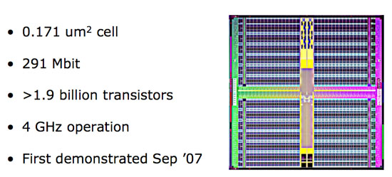
Intel's 32nm SRAM test vehicle
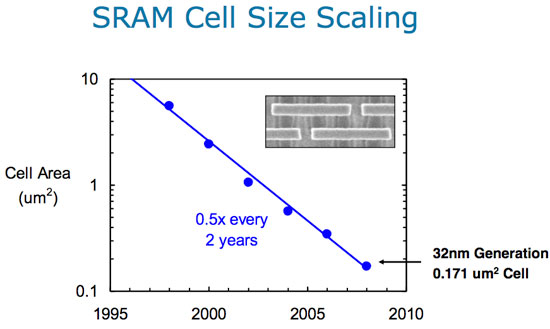
The 291Mbit chip was made up of over 1.9 billion transistors, switching at 4GHz, using Intel’s 32nm process. The important number to look at is the cell size, which is the physical area a single bit of cache will occupy. At 45nm that cell size was 0.346 um^2 (for desktop processors, Atom uses a slightly larger cell), compared to 0.370 um^2 for AMD’s 45nm SRAM cell size. At 32nm you can cut the area nearly in half down to 0.171 um^2 for a 6T SRAM cell. This means that in the same die area Intel can fit twice the cache, or the same amount of cache in half the area. Given that Core i7 is a fairly large chip at 263 mm^2 I’d expect Intel to take the die size savings and run with them. Perhaps with a modest increase to L3 cache size.
A big reason we’re even getting this disclosure today is because of how healthy the 32nm process is. Below we have a graph of defect density (number of defects in silicon per area) vs time; manufacturing can’t start until you’re at the lowest part of that graph - the tail that starts to flatten out:
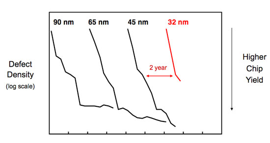
Intel’s 45nm process ramped and matured very well as you can see from the chart. The 45nm process reached lower defect densities than both 65nm and 90nm and did it faster than either process. Intel’s 32nm process is on track to outperform even that.
Two Different 32nm Processes?
With Intel now getting into the SoC business (System on a Chip), each process node will now have two derivatives - one for CPUs and one for SoCs. This started at 45nm with process P1266.8, used for Intel’s consumer electronics and Moorestown CPUs and will continue at 32nm with the P1269 process.
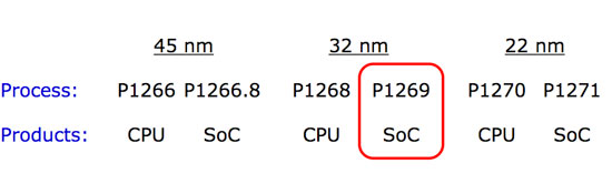
There are two major differences between the CPU and SoC versions of a given manufacturing process. One, the SoC version will be optimized for low leakage while the CPU version will be optimized for high drive current. Remember that graph comparing leakage vs. drive current of 45nm vs. 32nm? The P1268 process will exploit the arrows to the right, while P1269 will attempt to push leakage current down.
The second difference is that certain SoC circuits require higher than normal voltages and thus you need a process that can tolerate those voltages. Remember that with a SoC it’s not always just Intel IP being used, there are many third parties that will contribute to the chips that eventually make their way into smartphones and other ultra portable devices.
The buck doesn’t stop here, in two more years we’ll see the introduction of P1270, Intel’s 22nm process. But before we get there, there’s a little stop called Sandy Bridge. Let’s talk about microprocessors for a bit now shall we?


64 Comments
View All Comments
blyndy - Wednesday, February 11, 2009 - link
Let me see if I've got this straight: in 2H'09 (I would actually bet Q3'09) we will finally see the Core i5 quads-cores (Lynnfield/Clarksfield) (on a new LGA-1156 socket), which should have been released in Dec'08.So the 45nm Core i5 quads will be the highest performing CPU available for LGA-1156, positioning above the 32nm Clarkdale/Arrandale dual-cores (the 'Core i5 Duo' maybe?) which arrive in Q4'09
How do they indent to make the LGA-1366 platform have better overclockability, i7 and i5 are almost the same, are they going to actively prevent OC'ing on i5? that would be ridiculous.
Somehow I don't think that the artificial socket segmentation will have a significant number of enthusiast herded into LGA-1366 to get the higher margin cash-cow that Intel has planned it to be.
Triple Omega - Sunday, February 15, 2009 - link
Intel isn't going to artificially limit overclocking directly, but it is indirectly by redirecting the better chips to 1366. So the i7 CPU's will be cherry-picked versions of the i5's and thus will overclock better. Besides that the only socket with Extreme versions will be 1366.(Though that is a niche within a niche really)philosofool - Wednesday, February 11, 2009 - link
Overclockers are a very small fraction of the market. I'm not even sure intel is thinking about overclockability when they engineer chips. Overclockability is more an artefact of good engineering than a design goal from the outset. Overclockers are always paranoid that intel or AMD is out to get them by intentionally crippling chips. There just aren't enough of us for Intel to be concerned. We're like 1% of the total CPU market.Pretty much every chip that intel has released at any price point since the introduction of Core 2 has been wonderfully overclockable. I wouldn't worry that Intel is going to change that soon, especially since Core i5 is basically just mainstream processor with the same design fundamentals as the excellent i7.
JonnyDough - Wednesday, February 11, 2009 - link
Although I understand it's a hobby, I don't care if people can overclock or not. As long as we have fast chips at a good price and they're faster than what we have...I mean, why would you care? Isn't it all about SPEED?ssj4Gogeta - Wednesday, February 11, 2009 - link
i5 probably won't have an extreme version.Bezado11 - Wednesday, February 11, 2009 - link
I wouldn't be surprised if the opposite was true. I'm really sick of all the hype on shrinking creates less heat. Look at the gpu industry, ever since they started shrinking things got hotter and hotter, and now it seems with i7 even though it's not a die shrink and we are use to 45nm by now, the new hardware to support minor changes in architecture of the cpu seem to make things run hotter.I7 is way to hot. The newest GPU's run way to hot.
Lightnix - Thursday, February 12, 2009 - link
But you're making an unfair comparison - for example, the current latest GPUs have only been produced on the newest nodes, ever. Now, if we take for example, a Radeon 3870 vs. a Radeon 2900 XT, the former draws far less power and will overclock better on air, almost directly as a result of them shrinking from a 80nm to a 55nm process, despite them performing exactly the same. Another example is the Core 2 E8000 series and E6000 series. Despite the increase in cache size, the E8000 dissipates little enough heat that they can provide them with a very tiny heatsink compared to the earlier 65nm cores, and objectively they draw much less power at the same clock speed because they run at lower volts.You can see this sort of thing again and again throughout the technology industry, Coppermine (180nm) -> Tualatin(130nm), GeForce 7800 -> 7900, G80 -> G92, etc., etc.
If you were to compare say, a GTX280 to a 8800 GTX and say the former draws much more power than the 8800 GTX, AND it's produced on a smaller process - well, yes, but that's because they've clocked it higher and there are far more transistors (twice as many, in fact).
Mr Perfect - Thursday, February 12, 2009 - link
That's because every time they shrink the chips they pack in new features and push the clock speed to the bleeding edge. If all they did was die shrink the old tech, we'd all be running something like an Atom CPU right now. Atoms closely resemble Pentium 3s, but on modern manufacturing only draw what? 5 watts?V3ctorPT - Wednesday, February 11, 2009 - link
The GPU's run hotter, because they pack double the transistors with a new shrink, than their previous HW... Reduction of the manufacturing process enables that we can have so much more transistors in the same place, of course it gets hot...JonnyDough - Wednesday, February 11, 2009 - link
I think you need to re-read the manufacturing roadmap page. It details the leakage gain (heat).