Intel Unveils Meteor Lake Architecture: Intel 4 Heralds the Disaggregated Future of Mobile CPUs
by Gavin Bonshor on September 19, 2023 11:35 AM ESTCompute Tile: New P (Redwood Cove) and E-cores (Crestmont)
The compute tile is the first client-focused tile to be built on the Intel 4 process technology. It houses the latest-generation P-cores and E-cores, both of which are based on newer and updated architectures. The P-Cores are officially called Redwood Cove, while the E-Cores are Crestmont. Intel also claims that power efficiency is greatly improved from previous generations, combined with its 3D Foveros packaging and offloading less performance-critical elements such as the SoC, media, and graphics onto other tiles. Intel also uses the same ring fabric to interconnect all the tiles to reduce power and latency penalties across the entirety of the chip.
One thing to note with the new core architectures, including Redwood Cove (P-core) and Crestmont (E-core), is that Intel was very light on disclosing many of the finer details. While we got the general blurb of 'it's better than this and has better IPC performance than the last gen,' Intel has omitted details such as L3 cache, whether there's L4 cache through Intel's "Adamintine" hierarchy, and disclosing decoder widths within the cores. As such, Intel hasn't provided enough details for us to do a full architectural deep dive of Redwood Cove or Crestmot, but more an easy look to see what's new and how it's implemented.
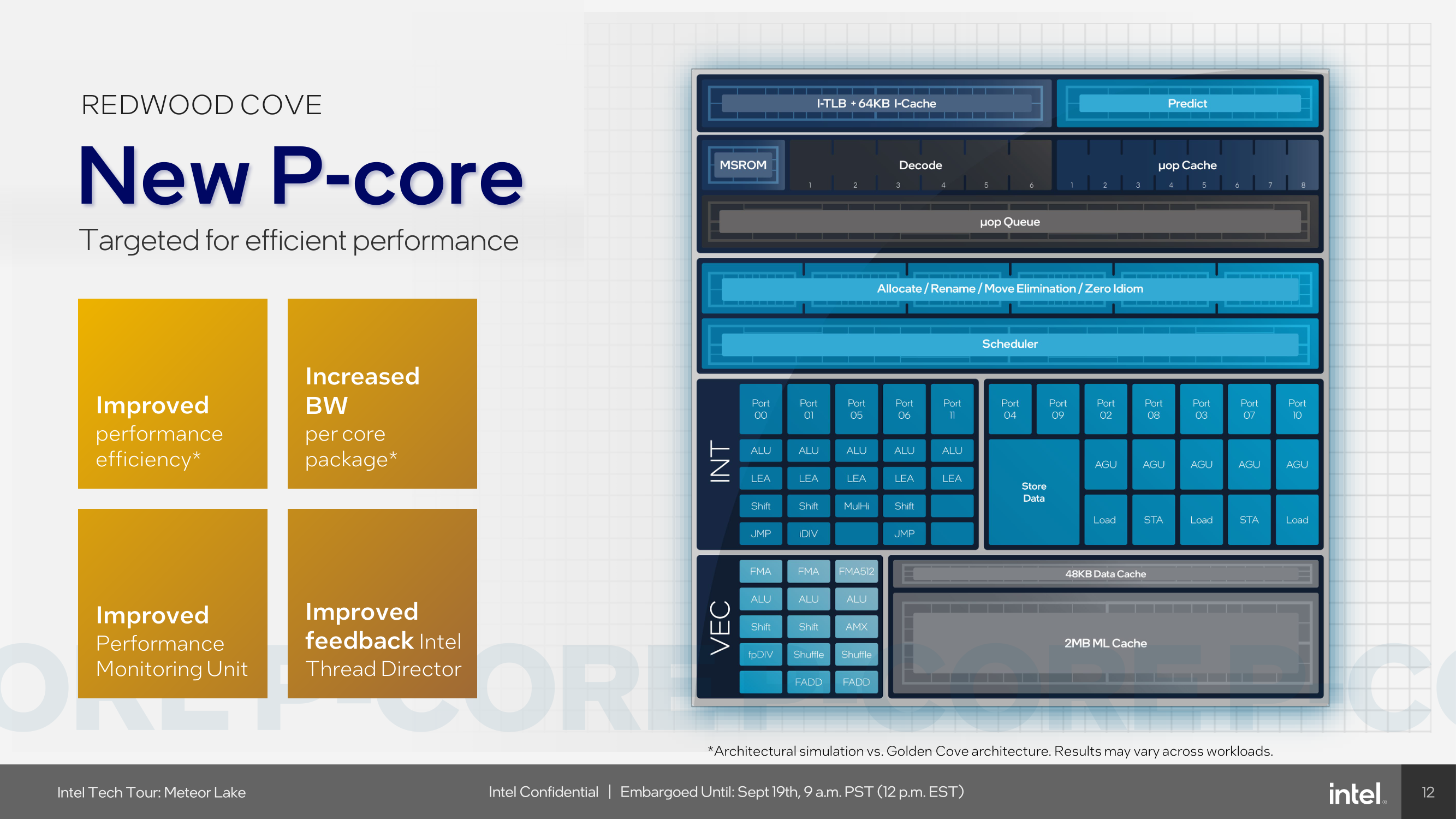
Looking at some of the new changes to Meteor Lake, one of the most notable is the introduction of the new Redwood Cove P-core. This new P-core is the direct successor to the previous Golden Cove core found in the 12th Gen Core (Raptor Lake) processors and is designed to bring generational improvements. As expected, Meteor Lake brings generational IPC gains through the new Redwood Cove cores. The Redwood Cove core also has increased bandwidth for both cache and memory. The performance monitoring unit has also been updated to enhance monitoring, and one of the standout features of the new P-Core is the enhanced feedback provided by Intel's Thread Director, which aids in optimizing core performance and directing workloads to the right cores.
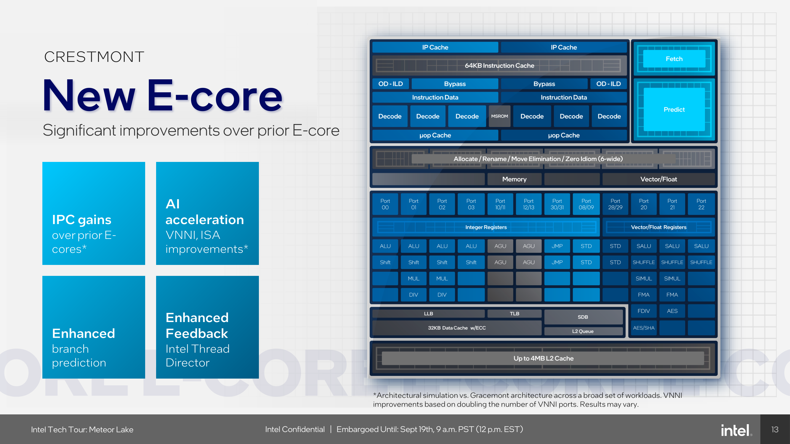
Another inclusion is the new Cresmont-based E-cores, which also benefit from generational IPC gains, and they keep the CPU-based AI acceleration through Vector Neural Network Instructions (VNNI) as seen on Raptor Lake (13th Gen) and Alder Lake (12th Gen). Intel claims improvements over the previous gens, although they haven't provided anything to substantiate this.
However, Intel states what it means by improvements: "Architectural simulation vs. Gracemont architecture across a broad set of workloads. VNNI improvements based on doubling the number of VNNI ports. Results may vary." This is a very roundabout way of saying we've doubled the number of AVX2 VNNI ports, but they haven't given us any figures, and with Raptor Lake, not all SKUs had support for the VNNI instruction set. They haven't told us whether or not this is now a feature of the Crestmont E-core itself or if it's, again, SKU-dependent.
This is designed to bolster the user experience when using AI applications and running AI-based workloads, although the NPU on the SoC tile is predominately more suited for these. Like the P-Cores, the E-Cores also benefit from enhanced Thread Director feedback, which provides better granular control and optimization. Workloads that aren't as intensive can be offloaded onto the new Low Power Island E-cores, which are embedded into the SoC tile.
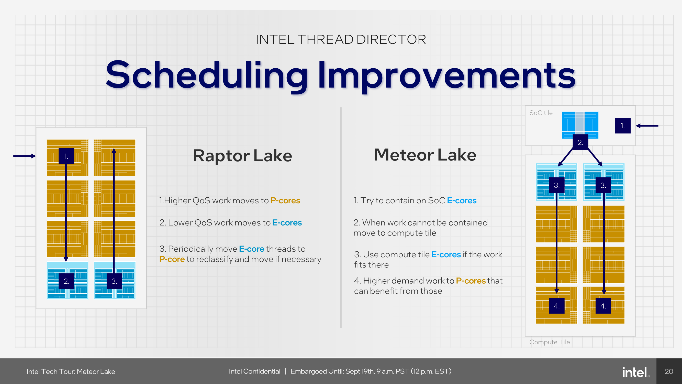
One area where Intel is promising major improvements and optimizations is through Thread Director. The Alder Lake (12th Gen) and Raptor Lake (13th Gen) architecture introduced a nuanced approach to scheduling. Under Alder/Raptor work was assigned a quality-of-service (QoS) ranking, and higher priority work was allocated to P-cores for more demanding and intensive workloads, while lower-ranked workloads are directed to E-cores, primarily to save power.
In cooperation with Microsoft Windows, Intel is bringing new enhancements and refinements into play for Meteor Lake. Meteor Lake's SoC tile LP E-cores represent a third tier of service, and Thread Director will try to keep work there first. Then, if threads need faster performance, they can be moved to the compute tile, accessing the faster, full-power E-cores, and at the top, the P-cores. This gives the chip better overall workload distribution in terms of power efficiency. Moreover, Meteor Lake's strategy to periodically move highly demanding tasks to the P-cores that can benefit from the higher performance levels offers a dynamic approach to thread scheduling.
Overall, this is designed to improve power efficiency through Meteor Lake, giving it more versatility over Raptor Lake regarding task scheduling. The flip side is that, on paper, Meteor Lake is a more efficient platform through these enhancements than Raptor Lake, especially in scenarios requiring rapid adjustments to fluctuating workloads and through those lighter workloads that can be offloaded onto the LP E-cores within the SoC.
Compute Tile: Intel 4 with EUV Lithography
The entirety of the compute tile, including the P and E-cores, is built using the Intel 4 node and is also Intel's first client chip to use EUV lithography. Intel 4 is a key part of Intel's IDM 2.0 strategy, which aims to achieve parity by 2024 and process leadership by 2025. We have already written a piece detailing the Intel 4 node in great detail, which can be found below:
Intel 4 Process Node In Detail: 2x Density Scaling, 20% Improved Performance
Intel 4 uses extreme ultraviolet (EUV) lithography, a highly efficient manufacturing technique that simplifies manufacturing, improving yield and area scaling. Not only is EUV, along with Intel 4, which is designed to scale out for better power efficiency, but it's also the precursor for Intel to switch things over to their Intel 3 process, which is still being developed.
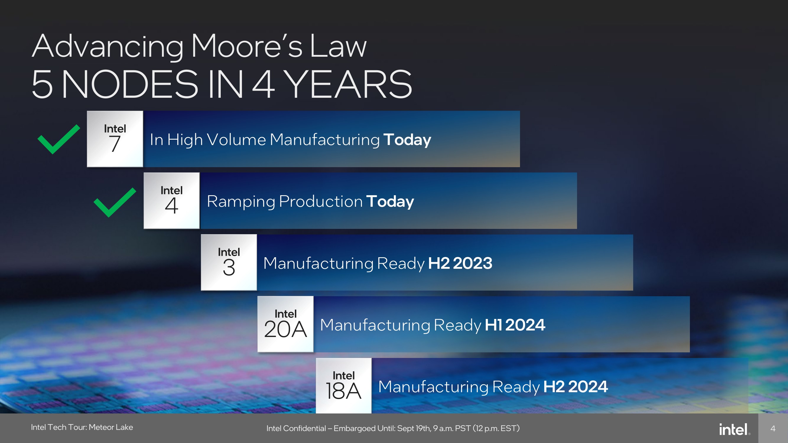
According to Intel's '5 nodes in 4 years' goal within the roadmap, Intel 3 is stated to be manufacturing-ready in H2 of 2023. What's interesting about the cadence of Intel 3 in the roadmap is that Intel 3 is design-compatible with Intel 4, and as such, Intel 3 is designed to be the long-lived node with EUV lithography.
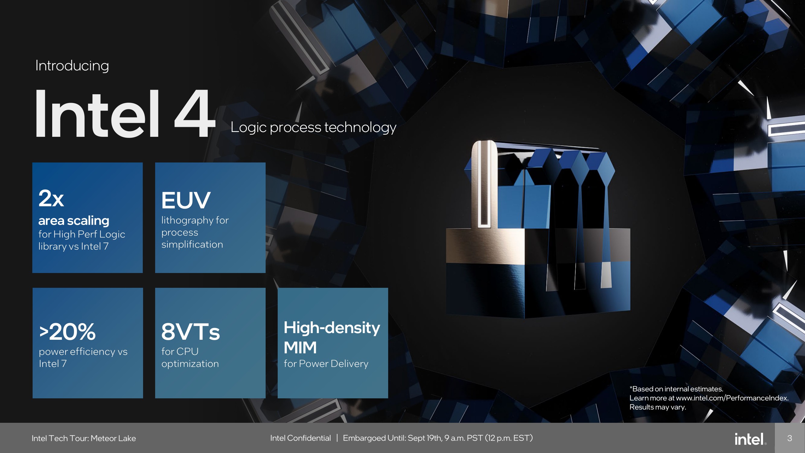
One of the primary benefits of Intel 4 is its area scaling capabilities. The Intel 4 process offers 2X the area scaling for high-performance logic libraries compared with the previous Intel 7 process node – a process which wasn't only troublesome through its exceedingly long development cycle, but yields were not the greatest. Having the ability to scale out in such a way is vital for fitting more and more transistors on a chip, which should theoretically improve the overall performance and efficiency of the silicon. Intel 4 is also optimized for high-performance computing applications and supports both low-voltage (<0.65V) and high-voltage (>1.1V) operations. Intel claims that having this flexibility results in more than 20% performance in iso-power performance over Intel 7, and the technology also incorporates high-density Metal-Insulator-Metal (MIM) capacitors, which Intel claims make power delivery to the chip superior.
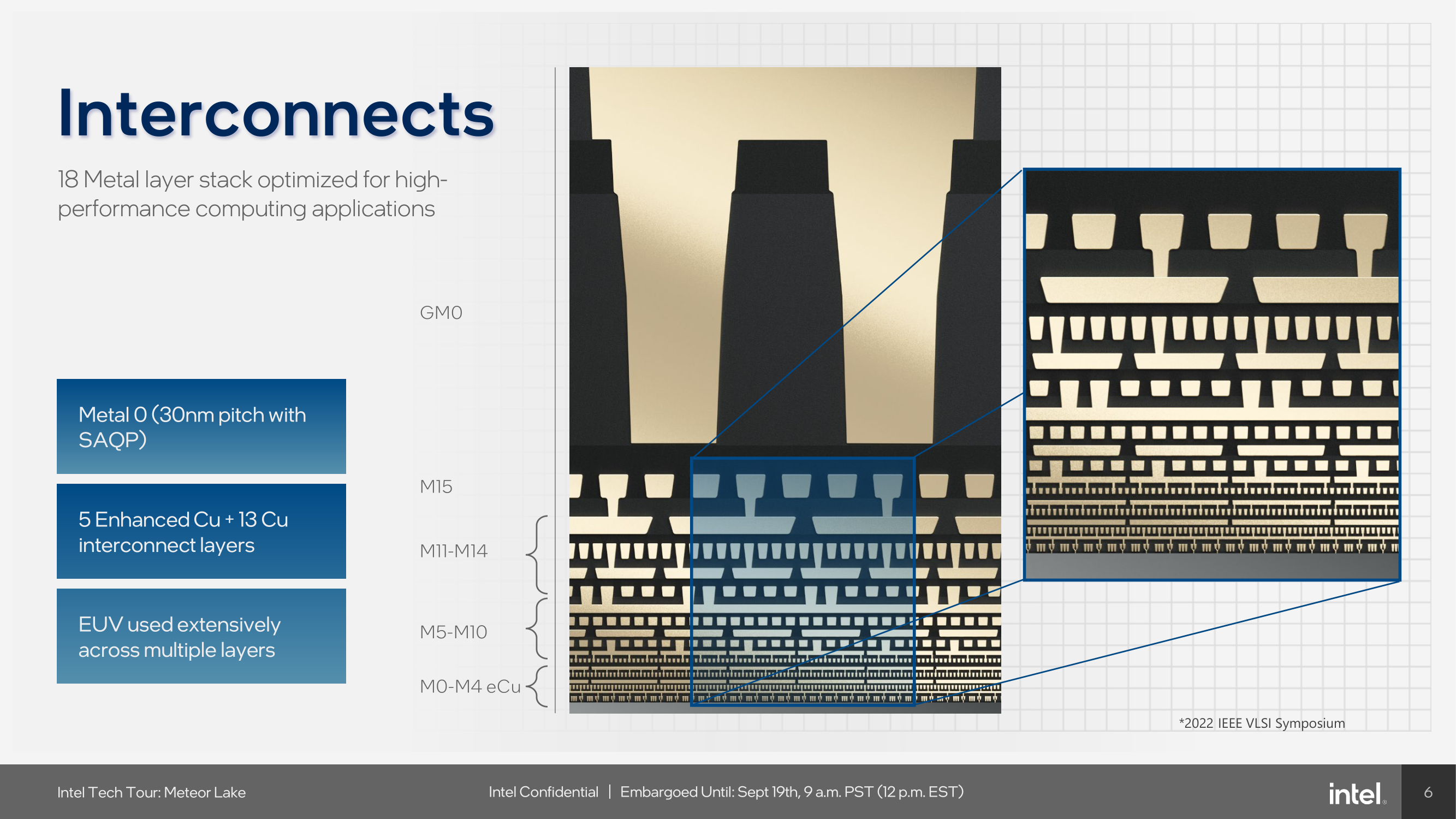
Through Intel 4 with EUV, Intel uses a 30 mm fin pitch with self-aligned quad patterning (SAQP) and a 50 nm tungsten gate pitch, scaled down by 0.83x from 54/60 nm on Intel 7. The M0 pitch is also down by 0.75x to 30 nm from 40 nm, and the HP library height has been reduced greatly from 408 in Intel 7 to 240 nm on Intel 4, a scaling of 0.59x. Moving from a 4 fin to 3 fin allocation means that Meteor Lake on Intel 4 has a tighter gate spacing than Intel 7.
One key new introduction to Intel 4 is the materials used, with Intel using what it calls 'Enhanced Copper'. Although Intel hasn't disclosed the specific percentage of the mixture, Enhanced Copper is essentially copper (Cu) adorned with cobalt (Co) and is designed to eliminate high resistance and high volume barriers. The combined metallurgy of copper and cobalt is used on layers M0 to M4, while layers M5 to M15 are made from copper using different pitches ranging from 50 nm up to 280 nm.
| Comparing Intel 4 to Intel 7 | |||
| Intel 4 | Intel 7 | Change | |
| Fin Pitch | 30 nm | 34 nm | 0.88 x |
| Contact Gate Poly Pitch | 50 nm | 54/60 nm | 0.83 x |
| Minimum Metal Pitch (M0) | 30 nm | 40 nm | 0.75 x |
| HP Library Height | 240h | 408h | 0.59 x |
| Area (Library Height x CPP) | 12K nm2 | 24.4K nm2 | 0.49 x |
Using Extreme Ultraviolet (EUV) lithography on Intel 4 represents a major progressive advancement in semiconductor fabrication. Accomplished by using x-rays with a wavelength of around 13.5 nanometers (generated by zapping tin with a laser, no less), EUV lithography significantly improves and optimizes the photolithographic process, allowing for enhanced resolution and pattern fidelity metrology. The technology requires specialized equipment, including high-precision optics and vacuum chambers, with a single EUV lithographic system costing around $150 million (as per Reuters).
When it comes to using manufacturing chips, there are different levels of patterning, both single and multi-patterning. Using EUV allows Intel to reduce the number of masks and steps in the fabrication process, with up to 20% fewer masks on Intel 4 than Intel 7 by replacing multi-patterning steps a single EUV layer. While each patterning level presents its own unique challenges, EUV allows for a single pattern to use just one exposure to etch out. This means that production can be increased and flow faster throughout the process. Opting for multi-patterning means more cost and higher variability. Another advantage of using a single-pattern EUV process also reduces the number of defects within the silicon.
Despite the substantial capital and operational expenditures, the technology offers compelling advantages, such as a reduction in mask count by 20% and a decrease in process steps by 5% for Intel 4. These efficiencies contribute to superior area scaling and yield optimization and put EUV lithography as a cornerstone in Intel's processor roadmap as they try to achieve leadership. It also synergizes with Advanced Packaging Technologies (APT) like Embedded Multi-die Interconnect Bridge (EMIB) and is combined with Foveros 3D packaging, further ensuring its role as a progressive technology in semiconductor and chip manufacturing.


107 Comments
View All Comments
PeachNCream - Thursday, September 21, 2023 - link
Nice trolling lemur! You landed like an entire page of nerd rage this time. You're a credit to your profession and if I could give you an award for whipping dead website readers into a frenzy (including regulars who have seen you do this for years now) I would. Congrats! 10/10 would enjoy again.IUU - Thursday, September 28, 2023 - link
Intel does not need to do anything about its architecture to to match or surpass m3. It just needs to build its cpus on a similar node. Which is not happening anytime soon, thus perpetuating the illusion of efficiency of apple cpus.Two things more. First it is hilarious to compare the prowess of Intel on designing cpus to that of Apple. Apple has long time "building" machines like a glorified Dell borrowing cpus from IBM or Intel and only recently understood the scale and effort needed to design your silicon by improving on ARM designs.
Secondly, it is misguided to say that if a cpu needs 10 times more wattage on the same node to achieve 2 or 3 times the performance is less efficient. This is not how physics works . If Intel built their cpus on N3 of tsmc they would be 2 or 3 times faster best case scenario. Wattage does not scale linearly with performance. This is the same as saying that a car that has 10 times the power would be 10 times faster. Lololol.
Apple designs good cpus recently , but all the hype about its efficiency is just hype. Even if we assume the design is totally coming from Apple , which it doe not, being a very good modification at best, it does not even build its nodes. By large its efficiency is TSMC efficiency. If it were not for TSMC Apple would be non existent on the performance charts.
Silma - Tuesday, September 19, 2023 - link
TLDR:- Intel 4 < TSMC N6
- To not be late, Intel 3 must arrive within 3 months,which is highly doubtful, since Intel 4 isn't even shipping yet
- I assume Intel 3 < TSMC N6, otherwise, why bother enriching the competition?
- Parts of the new tech stack looks promising, but Intel refrains from any real performance claims, or any comparison with offerings from AMD or Apple.
- Did Intel announce another architecture for desktop computers, probably more similar to that of AMD, e.g. perhaps many performance tiles plus one cache tile?
Drumsticks - Tuesday, September 19, 2023 - link
Maybe. Or maybe TSMC6 is cheaper, and Intel doesn't need the power savings or area savings of I4 over TSMC6 for what the non-compute tiles need to accomplish. It's not exactly uncommon to see the SoC / IO tile on a lower node, doesn't AMD do the same thing?Roy2002 - Tuesday, September 19, 2023 - link
Intel 4 and 3 are basically the same with the same device density as 3 is enhanced 4. I assume it has slightly higher density value than TSMC 5nm and performance is slightly better. Let's see.kwohlt - Tuesday, September 19, 2023 - link
Intel 4 is not library complete. It can't be used for the SoC tile.sutamatamasu - Tuesday, September 19, 2023 - link
I wonder if current processor have an dedicated NPU, then what the heck happen with GNA?It still in there or they're remove it?
Exotica - Tuesday, September 19, 2023 - link
Intel should've either implemented TB5 in Meteor Lake or waited until after Meteor Lake shipped to announce TB5. Because as cool and impressive as meteor lake seems, for some of us, it's already obsolete in that it makes no sense to buy a TB4 laptop/PC and instead wait on TB5 silicon to hit the market.FWhitTrampoline - Tuesday, September 19, 2023 - link
Why use TB4 or USB4/40Gbs and have to deal with the extra latency and bandwidth robbing overhead compared to PCI-SIG's OCuLink that's just pure PCIe signalling delivered over an external OCuLink Cable. OCuLink and PCIe requires no extra protocol encapsulation and encoding/decoding steps at the PCIe link stage so that's lower latency there compared to USB4/TB4 and later generations that have to have extra encoding/decoding of any PCIe protocol packets to send that out over TB4/USB4. And for external GPUs 4 lanes of PCIe 4.0 connectivity can provide up to 64Gbs of bandwidth over an OCuLink port/cable and OCuLonk ports can be 8 PCIe lanes and wider there.Once can obtain an M.2/NVMe slot to OCuLink adapter and get an external OCuLink connection of up to 64Gbs as long as the M.2 is 4, PCIe 4.0 lanes wide and no specialized controller chip required on the MB to drive that. And GPD on their Handhelds offers a dedicated OCuLiink port and an external portable eGPU that supports OCuLink or USB4/40Gbs-TB interfacing. TB5 and USB4-V2 will take years to be adopted whereas OCuLink is just PCIe 3.0/4.0 there delivered over an external cable.
Exotica - Tuesday, September 19, 2023 - link
Unlike thunderbolt, Occulink doesn't have hotplugging, meaning your device must be connected at cold boot. Not so good for external storage needs.