Intel Unveils Meteor Lake Architecture: Intel 4 Heralds the Disaggregated Future of Mobile CPUs
by Gavin Bonshor on September 19, 2023 11:35 AM ESTGraphics Tile: A Generational Leap Through Arc, Xe-LPG Graphics
As part of their disaggregated architecture for Meteor Lake, Intel has opted to use a separate tile for graphics. Intel has gone down an interesting route for its disaggregated graphics, with the most notable inclusion through an upgrade to Intel's Arc Graphics architecture. Powering Intel's integrated graphics for Meteor Lake is a new graphics architecture which Intel calls Xe-LPG (and no, we're not talking about fuel here). Based on Intel's current discrete graphics architecture known as Xe-HPG (used in their Arc GPUs), Intel claims 2x performance per watt compared to the Xe-LP architecture-based Iris Xe integrated graphics within Intel's 12th Gen Core series.
There are a number of different elements within the graphics and media area of Meteor Lake, the bulk of which is built into the graphics tile, where the Xe-LPG graphics architecture is located. Unlike the compute tile (Intel 4) and the SoC tile, which is manufactured on TSMC N6 (6 nm), the graphics tile is made on TSMC's N5 node (5 nm), the same generational family as the nodes used by AMD and NVIDIA's discrete and integrated GPUs.
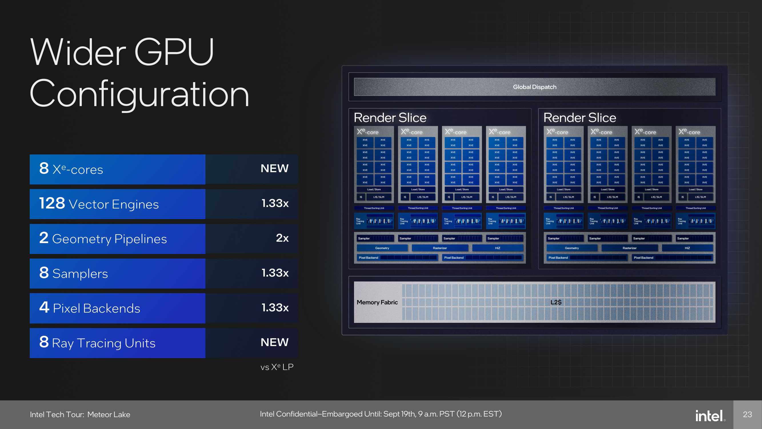
With Meteor Lake and the graphics tile with the Xe-LPG graphics processor, Intel is promising discrete-level performance in an integrated form factor. Looking at the finer specifications, Intel includes 8 x Xe graphics cores with 128 vector engines (12 per Xe core) and 8 samplers, representing a 1.33 x increase over Intel's previous Xe LP graphics. There are also 4 Pixel backends, which is an improvement over the 3 PBs on Xe LP. Intel also doubles the number of geometry pipelines within Xe-LPG, with two, and they also introduce 8 dedicated Ray Tracing Units (RTU), which is new for Intel's integrated graphics line-up.
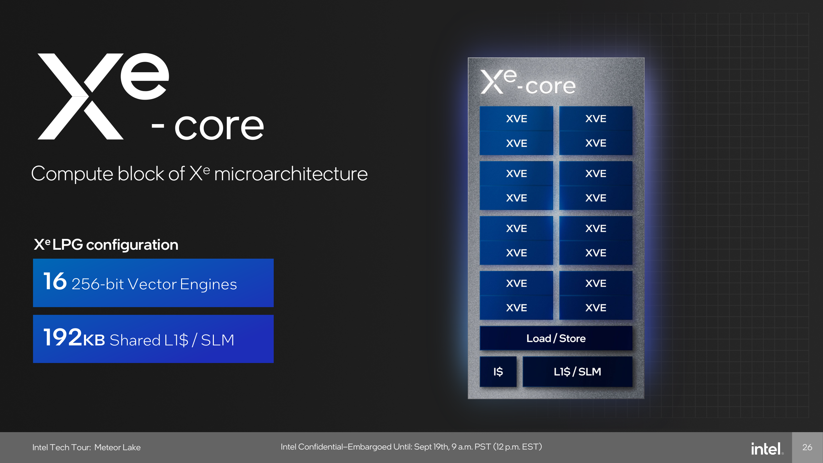
Looking at the makeup of Intel's Xe core, as previously mentioned, there are 16 Vector Engines that have a bus width of 256-bit, while each core also has 192 KB of shared L1 cache. Each Vector Engine enables 16 FP32 ops per clock, and 32 FP16 ops per clock, with a shared FP64 execution port with 64 INT8 ops per clock. One dedicated FP64 ops per clock unit is new over what's previously been seen in Raptor Lake and shares the overall design philosophy of Meteor Lake on power efficiency; pairs of Vector Engines can run in lockstep for better efficiency.
As part of Intel's goal of advancing the overall experience with Xe-LPG for users, the graphics are DX12 optimized, and Intel now brings Out of Order Samplng (OoOS) to Xe-LPG. It's worth noting that when talking about Execution Units (EUs), Intel's new and current term for this is Xe Vector Engines, or XVE for short. Intel hasn't provided us with how OoOS works within Xe-LPG, but we've reached out for more details.
| Comparing Intel Xe Integrated Graphics (Mobile) | ||||
| Meteor Lake (Xe-LPG) |
Raptor Lake (Xe-LP) |
Alder Lake GT1 (Xe-LP) |
Tiger Lake GT2 (Xe-LP) |
|
| Process Node | TSMC N5 | Intel 7 | Intel 7 | Intel 7 |
| Vector Engines/EUs | 128 | 96 | 96 | 96 |
| ALUs/Shaders | 1024 | 768 | 768 | 768 |
| TMUs | ?* | 48 | 16 | 48 |
| ROPs | ?* | 24 | 8 | 24 |
| Ray Tracing Units | 8 | - | - | - |
| TDP | ? | 15 W | 15 W | 15 W |
*Intel hasn't given us a deep dive into the finer specifications of Xe-LPG integrated graphics. Looking at an existing integrated Intel Arc equivalent with similar specs, the Meteor Lake Xe LPG could have 64 TMUs and 32 ROPs per the Arc A370M, which also has 1024 ALUs.
Comparing Intel's integrated Xe graphics from previous mobile architectures, Meteor Lake, through the Xe-LPG Arc based graphics, has 128 XVEs, which is an increase of 1.33 X or 32 XVE/EUs, than the previous Xe-LP generation. Regarding arithmetic logic units (ALUs), which are essentially shader cores, Xe-LPG has been increased to 1024, which is 128 ALUs per Xe-LPG core. As previously mentioned, Intel hasn't given us more about the finer specifications, including TMUs or ROPs, but does bring 8 Ray Tracing units, which is new for Xe-LPG when compared directly to Xe-LP.
Meanwhile, with Intel's Foveros 3D packaging technology, disaggregating the Media Engine and Display Engine from the graphics tile means when doing encoding or decoding, as well as video playback, it doesn't require the graphics tile to be powered up to do workloads on more power consuming cores.
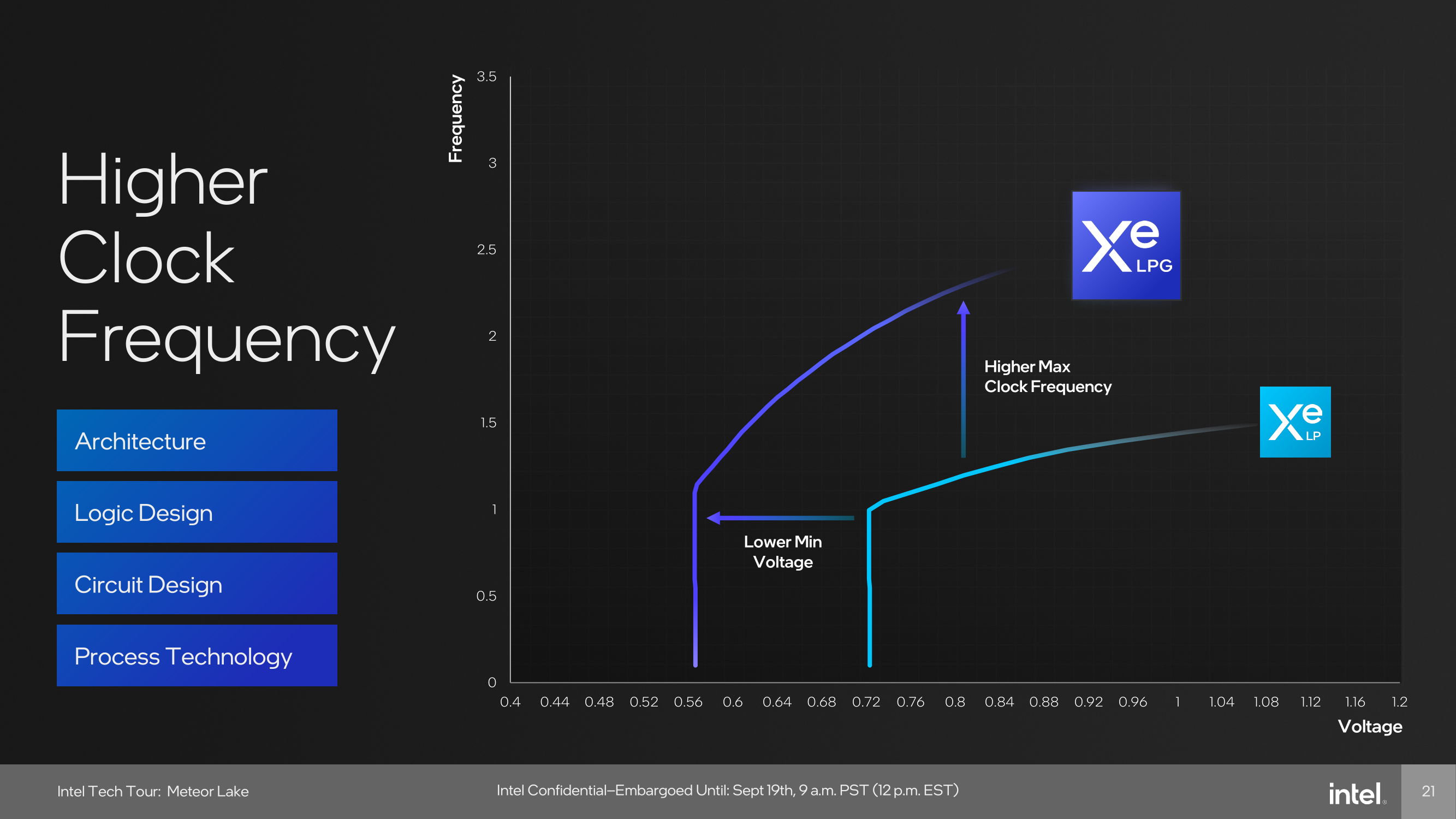
Intel Xe-LPG is the next step up from Xe LP, and one area where performance and efficiency gains are made is through a lower voltage frequency (V/F) curve, allowing the graphics to run at a lower minimum voltage with a higher maximum core clock speed. Intel has also optimized the pipelines for faster frequencies and is claiming up to 2 x performance at iso-voltages, which for a mobile platform such as Meteor Lake, adds more potential with a key focus on achieving a figure of up to 20% in power savings compared to the previous generation.


107 Comments
View All Comments
PeachNCream - Thursday, September 21, 2023 - link
Nice trolling lemur! You landed like an entire page of nerd rage this time. You're a credit to your profession and if I could give you an award for whipping dead website readers into a frenzy (including regulars who have seen you do this for years now) I would. Congrats! 10/10 would enjoy again.IUU - Thursday, September 28, 2023 - link
Intel does not need to do anything about its architecture to to match or surpass m3. It just needs to build its cpus on a similar node. Which is not happening anytime soon, thus perpetuating the illusion of efficiency of apple cpus.Two things more. First it is hilarious to compare the prowess of Intel on designing cpus to that of Apple. Apple has long time "building" machines like a glorified Dell borrowing cpus from IBM or Intel and only recently understood the scale and effort needed to design your silicon by improving on ARM designs.
Secondly, it is misguided to say that if a cpu needs 10 times more wattage on the same node to achieve 2 or 3 times the performance is less efficient. This is not how physics works . If Intel built their cpus on N3 of tsmc they would be 2 or 3 times faster best case scenario. Wattage does not scale linearly with performance. This is the same as saying that a car that has 10 times the power would be 10 times faster. Lololol.
Apple designs good cpus recently , but all the hype about its efficiency is just hype. Even if we assume the design is totally coming from Apple , which it doe not, being a very good modification at best, it does not even build its nodes. By large its efficiency is TSMC efficiency. If it were not for TSMC Apple would be non existent on the performance charts.
Silma - Tuesday, September 19, 2023 - link
TLDR:- Intel 4 < TSMC N6
- To not be late, Intel 3 must arrive within 3 months,which is highly doubtful, since Intel 4 isn't even shipping yet
- I assume Intel 3 < TSMC N6, otherwise, why bother enriching the competition?
- Parts of the new tech stack looks promising, but Intel refrains from any real performance claims, or any comparison with offerings from AMD or Apple.
- Did Intel announce another architecture for desktop computers, probably more similar to that of AMD, e.g. perhaps many performance tiles plus one cache tile?
Drumsticks - Tuesday, September 19, 2023 - link
Maybe. Or maybe TSMC6 is cheaper, and Intel doesn't need the power savings or area savings of I4 over TSMC6 for what the non-compute tiles need to accomplish. It's not exactly uncommon to see the SoC / IO tile on a lower node, doesn't AMD do the same thing?Roy2002 - Tuesday, September 19, 2023 - link
Intel 4 and 3 are basically the same with the same device density as 3 is enhanced 4. I assume it has slightly higher density value than TSMC 5nm and performance is slightly better. Let's see.kwohlt - Tuesday, September 19, 2023 - link
Intel 4 is not library complete. It can't be used for the SoC tile.sutamatamasu - Tuesday, September 19, 2023 - link
I wonder if current processor have an dedicated NPU, then what the heck happen with GNA?It still in there or they're remove it?
Exotica - Tuesday, September 19, 2023 - link
Intel should've either implemented TB5 in Meteor Lake or waited until after Meteor Lake shipped to announce TB5. Because as cool and impressive as meteor lake seems, for some of us, it's already obsolete in that it makes no sense to buy a TB4 laptop/PC and instead wait on TB5 silicon to hit the market.FWhitTrampoline - Tuesday, September 19, 2023 - link
Why use TB4 or USB4/40Gbs and have to deal with the extra latency and bandwidth robbing overhead compared to PCI-SIG's OCuLink that's just pure PCIe signalling delivered over an external OCuLink Cable. OCuLink and PCIe requires no extra protocol encapsulation and encoding/decoding steps at the PCIe link stage so that's lower latency there compared to USB4/TB4 and later generations that have to have extra encoding/decoding of any PCIe protocol packets to send that out over TB4/USB4. And for external GPUs 4 lanes of PCIe 4.0 connectivity can provide up to 64Gbs of bandwidth over an OCuLink port/cable and OCuLonk ports can be 8 PCIe lanes and wider there.Once can obtain an M.2/NVMe slot to OCuLink adapter and get an external OCuLink connection of up to 64Gbs as long as the M.2 is 4, PCIe 4.0 lanes wide and no specialized controller chip required on the MB to drive that. And GPD on their Handhelds offers a dedicated OCuLiink port and an external portable eGPU that supports OCuLink or USB4/40Gbs-TB interfacing. TB5 and USB4-V2 will take years to be adopted whereas OCuLink is just PCIe 3.0/4.0 there delivered over an external cable.
Exotica - Tuesday, September 19, 2023 - link
Unlike thunderbolt, Occulink doesn't have hotplugging, meaning your device must be connected at cold boot. Not so good for external storage needs.