Intel Unveils Meteor Lake Architecture: Intel 4 Heralds the Disaggregated Future of Mobile CPUs
by Gavin Bonshor on September 19, 2023 11:35 AM ESTGraphics Tile: A Generational Leap Through Arc, Xe-LPG Graphics
As part of their disaggregated architecture for Meteor Lake, Intel has opted to use a separate tile for graphics. Intel has gone down an interesting route for its disaggregated graphics, with the most notable inclusion through an upgrade to Intel's Arc Graphics architecture. Powering Intel's integrated graphics for Meteor Lake is a new graphics architecture which Intel calls Xe-LPG (and no, we're not talking about fuel here). Based on Intel's current discrete graphics architecture known as Xe-HPG (used in their Arc GPUs), Intel claims 2x performance per watt compared to the Xe-LP architecture-based Iris Xe integrated graphics within Intel's 12th Gen Core series.
There are a number of different elements within the graphics and media area of Meteor Lake, the bulk of which is built into the graphics tile, where the Xe-LPG graphics architecture is located. Unlike the compute tile (Intel 4) and the SoC tile, which is manufactured on TSMC N6 (6 nm), the graphics tile is made on TSMC's N5 node (5 nm), the same generational family as the nodes used by AMD and NVIDIA's discrete and integrated GPUs.
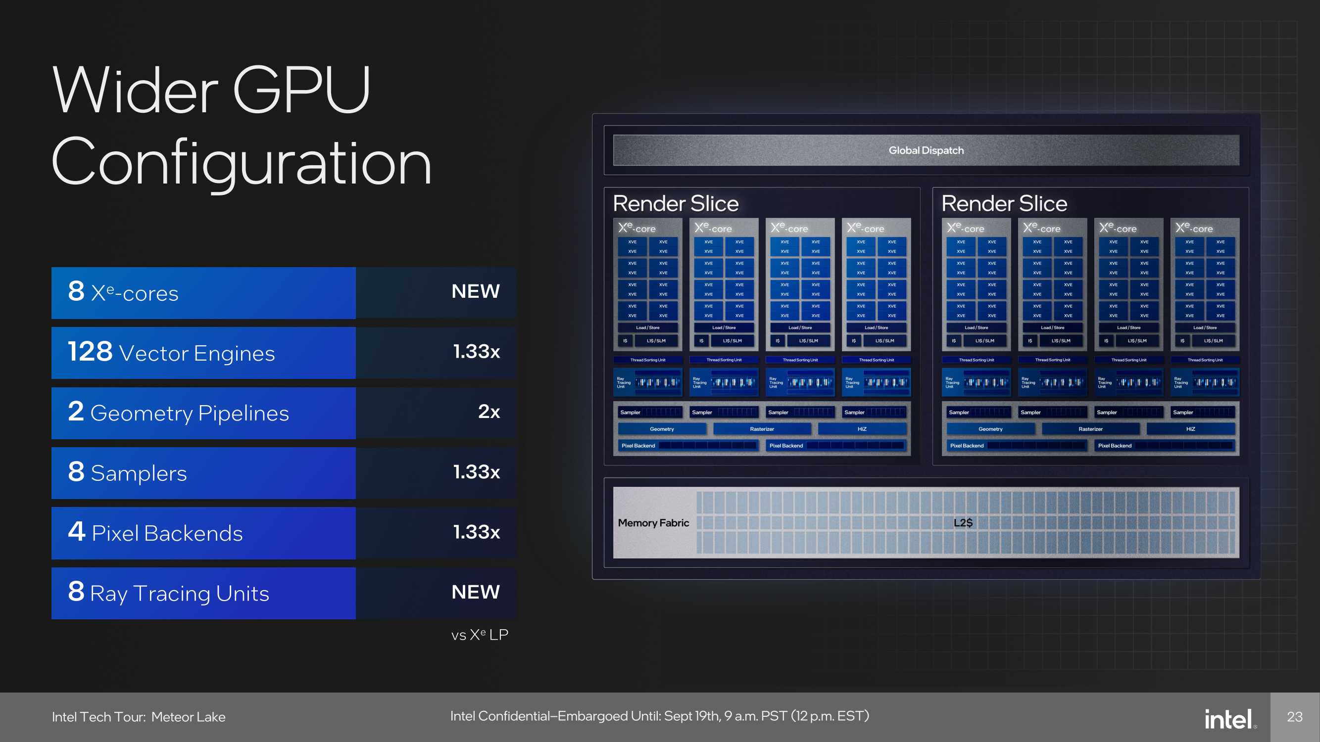
With Meteor Lake and the graphics tile with the Xe-LPG graphics processor, Intel is promising discrete-level performance in an integrated form factor. Looking at the finer specifications, Intel includes 8 x Xe graphics cores with 128 vector engines (12 per Xe core) and 8 samplers, representing a 1.33 x increase over Intel's previous Xe LP graphics. There are also 4 Pixel backends, which is an improvement over the 3 PBs on Xe LP. Intel also doubles the number of geometry pipelines within Xe-LPG, with two, and they also introduce 8 dedicated Ray Tracing Units (RTU), which is new for Intel's integrated graphics line-up.
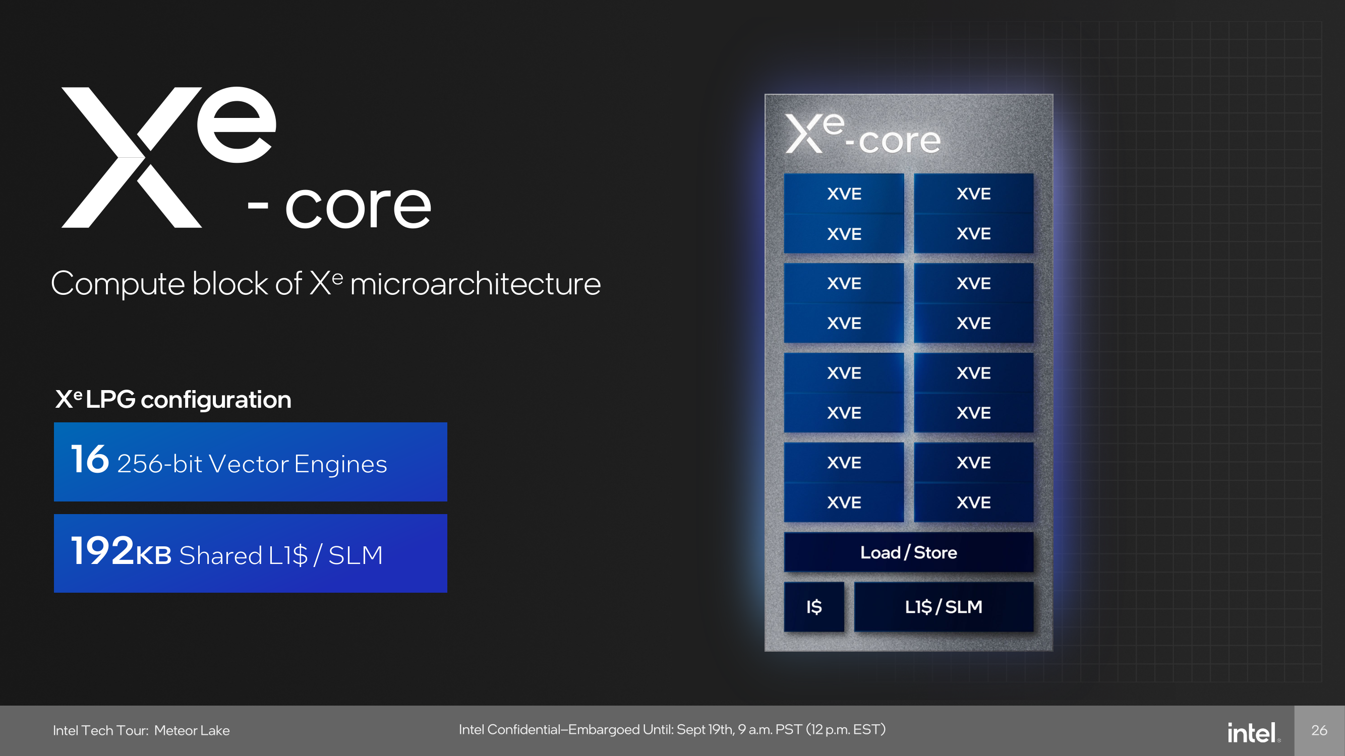
Looking at the makeup of Intel's Xe core, as previously mentioned, there are 16 Vector Engines that have a bus width of 256-bit, while each core also has 192 KB of shared L1 cache. Each Vector Engine enables 16 FP32 ops per clock, and 32 FP16 ops per clock, with a shared FP64 execution port with 64 INT8 ops per clock. One dedicated FP64 ops per clock unit is new over what's previously been seen in Raptor Lake and shares the overall design philosophy of Meteor Lake on power efficiency; pairs of Vector Engines can run in lockstep for better efficiency.
As part of Intel's goal of advancing the overall experience with Xe-LPG for users, the graphics are DX12 optimized, and Intel now brings Out of Order Samplng (OoOS) to Xe-LPG. It's worth noting that when talking about Execution Units (EUs), Intel's new and current term for this is Xe Vector Engines, or XVE for short. Intel hasn't provided us with how OoOS works within Xe-LPG, but we've reached out for more details.
| Comparing Intel Xe Integrated Graphics (Mobile) | ||||
| Meteor Lake (Xe-LPG) |
Raptor Lake (Xe-LP) |
Alder Lake GT1 (Xe-LP) |
Tiger Lake GT2 (Xe-LP) |
|
| Process Node | TSMC N5 | Intel 7 | Intel 7 | Intel 7 |
| Vector Engines/EUs | 128 | 96 | 96 | 96 |
| ALUs/Shaders | 1024 | 768 | 768 | 768 |
| TMUs | ?* | 48 | 16 | 48 |
| ROPs | ?* | 24 | 8 | 24 |
| Ray Tracing Units | 8 | - | - | - |
| TDP | ? | 15 W | 15 W | 15 W |
*Intel hasn't given us a deep dive into the finer specifications of Xe-LPG integrated graphics. Looking at an existing integrated Intel Arc equivalent with similar specs, the Meteor Lake Xe LPG could have 64 TMUs and 32 ROPs per the Arc A370M, which also has 1024 ALUs.
Comparing Intel's integrated Xe graphics from previous mobile architectures, Meteor Lake, through the Xe-LPG Arc based graphics, has 128 XVEs, which is an increase of 1.33 X or 32 XVE/EUs, than the previous Xe-LP generation. Regarding arithmetic logic units (ALUs), which are essentially shader cores, Xe-LPG has been increased to 1024, which is 128 ALUs per Xe-LPG core. As previously mentioned, Intel hasn't given us more about the finer specifications, including TMUs or ROPs, but does bring 8 Ray Tracing units, which is new for Xe-LPG when compared directly to Xe-LP.
Meanwhile, with Intel's Foveros 3D packaging technology, disaggregating the Media Engine and Display Engine from the graphics tile means when doing encoding or decoding, as well as video playback, it doesn't require the graphics tile to be powered up to do workloads on more power consuming cores.
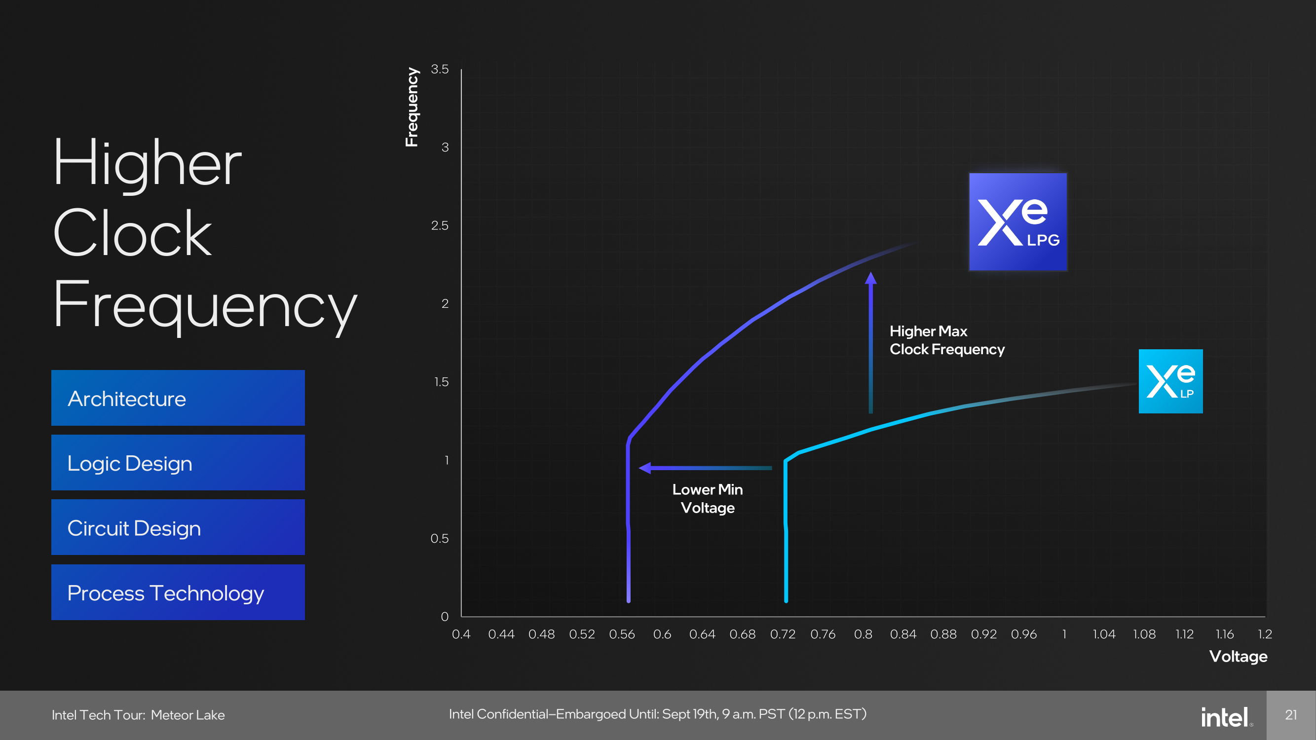
Intel Xe-LPG is the next step up from Xe LP, and one area where performance and efficiency gains are made is through a lower voltage frequency (V/F) curve, allowing the graphics to run at a lower minimum voltage with a higher maximum core clock speed. Intel has also optimized the pipelines for faster frequencies and is claiming up to 2 x performance at iso-voltages, which for a mobile platform such as Meteor Lake, adds more potential with a key focus on achieving a figure of up to 20% in power savings compared to the previous generation.


107 Comments
View All Comments
Composite - Thursday, September 28, 2023 - link
totally agree. At the same time, instead of doing a full Intel 4 Meteor lake chip, shrink it down to compute tile only also reduces the size of the silicon and improves yield. Later next year, Intel will also need EUV capacity for Sierra Forest and Granite Rapids. These chips will be much larger than mobile compute tile and considerably lower yield.... Intel will need every ounce of EUV capacity they have.tipoo - Tuesday, September 19, 2023 - link
Probably to have as much compute on the N4 capacity that they have, their substrate also takes much less power connecting them than current AMD and it allows for the best node for each part being used i.e if Intel's wasn't ideal for the GPU tile as the CPU tile etcComposite - Thursday, September 28, 2023 - link
I have the same question. At the same time, I was curious about Intel's EUV capacity. Since Intel is the late comer to EUV and over 50% of EUV machines are at TSMC, does Intel really have the capacity to manufacture full chip Intel 4 Meteor Lake? Not to mention up coming Sierra Forest and later on Granite Rapids will all use EUV capacity. I think the reasonable way is indeed only use EUV at the most critical part of Meteor Lake ---> Compute tile, and out source the rest.eSyr - Tuesday, September 19, 2023 - link
To avoid the issues they have with rollout 14 nm (BDW) and then 10 nm (CNL), I guess, when they held back by yield with respect to particular parts of the chip, specifically, GPU.lemurbutton - Tuesday, September 19, 2023 - link
A17 Pro just beat all Intel CPUs except the 13900KS in ST Geekbench6. A17 Pro uses less than 3w to achieve this - with typical load significantly below 3w. Meanwhile, 13900KS uses as much as 250w or more.Intel's Meteor Lake needs to improve by 10x over Raptor Lake just to match what M3 will be able to do.
Irish_adam - Tuesday, September 19, 2023 - link
The 13900ks uses 250 watts on a single core? Got a link for that?I'll think you find that single core workloads use far, far less. Also remember that benchmarks across ISA's are sketch at best and outright made up at worst. I mean just look how badly games or software can be when ported from one ISA to another, it all really comes down to how well you've made the software to run on each architecture.
Makaveli - Tuesday, September 19, 2023 - link
He is an apple fanboySource: Trust me bro!
FWhitTrampoline - Tuesday, September 19, 2023 - link
No the A17 Performance core is only clocked at 3.6/3.7GHz compared to the x86 designs that are up to clocked 2Ghz+ higher. So this is not some ESPN like Fanatic statement as since the A14/Firestorm core Apple's instruction decoder width is at least 8 decoders wide and backed up by loads of execution ports. And so Apple's P cores are of a very wide order superscalar design since the A14/Firestorm was released!And the Apple P cores are high IPC at low clocks compared to the x86 designs that have 4/6 instruction decoders so need the higher clocks to make up the IPC deficiency for single thread performance that's calculated as IPC multiplied by average sustained clocks to get that single threaded performance metric.
The lower clocks are where Apple's power savings come from and the longer battery life is obtained. That and the A17 Pro/Earlier A series SOCs have loads of specialized heterogeneous compute for offloading workloads onto instead of using the CPU cores or GPU cores so more power can be saved there for all sorts of specialized workloads. The x86 processors/SOCs are just now getting the same sorts of specialized heterogeneous compute IP blocks but that's relatively immature compare to Apple's SOCs and other ARM Based SOC ecosystems that have been using that specialized heterogeneous compute IP for years now.
GeoffreyA - Thursday, September 21, 2023 - link
Well, it would be interesting to see Intel or AMD make a fixed-width ISA design and how that then stacks up against the stuff of Apple. Really, x86 is at a disadvantage because of the variable-width instructions but still has done a fantastic job. Or, I'd like to see Apple design an x86 CPU and see how that holds up against Zen and the rest.FWhitTrampoline - Thursday, September 21, 2023 - link
No logical reason for Apple to go CISC as the x86 Instruction Decoder requires many times the transistors to implement than the transistors required to implement a RISC ISA Instruction Decoder! So it was easy to get 8 Instruction Decoders to fit on the front of the A14/Firestorm processor core(RISC ISA Based). It's easier to go wider if one has a relatively fewer Instructions of a fixed length to implement in a Instruction Decoder design. So that makes it easy to produce a custom very wide order superscalar processor core design that targets high IPC at a lower clock rate and the SOC's CPU cores clocked well inside their Performance/Watt sweet spot. And to still have that A14 match/get close to the x86 cores in single threaded performance and against x86 core designs that are clocked 2GHz+ higher.The x86 ISA is too Legacy Instructions bloated and it's not going to be easy to refactor that and not require years in the process to do that. The ARM ISA ecosystem is from the ground up RISC there and even though the x86 designers have a RISC like back end to break those CISC down into more RISC like instructions, that hardware engine take more transistors to implement and thus will use more power resources getting that done. The vast majority of ARM ISA instructions translate 1 to 1 into single and some a few Micro-OPs so how hard is that to decode compared to x86 ISA instruction that mostly have multiple micro-ops generated to get all that complex work done. And there's a valid power usage reason that x86 never made any inroads into the wider tablet/smartphone market.
The thing about the ARM/RISC core designs is that they can scale from phones to server/HPC whereas the CISC designs can not scale down as low power as RISC designs! but Intel has done a good job at getting close there but a little too late to matter to the OEMs that really did not want to remain beholden to Intel and x86. And the same can be said now for RISC-V compared to an ARM Holdings that's maybe leaning more towards an x86 like business model where RISC-V represents total end user ISA freedom there, within reason, as the RISC-V ISA is totally open not royalist/encumberments required/enforced.