Intel Unveils Meteor Lake Architecture: Intel 4 Heralds the Disaggregated Future of Mobile CPUs
by Gavin Bonshor on September 19, 2023 11:35 AM ESTSoC Tile, Part 3: Disaggregating Xe Media and Display Engine From Graphics
As we noted earlier, Intel has completely redesigned its graphics, media, and display engine for Meteor Lake and, as such, separates all three entities from each other. While we'll cover the new graphics tile next, we'll start with everything that's not part of the graphics tile. Opting for a disaggregated architecture allows Intel to not only shuffle things around from an IP perspective but also allows Intel to integrate new IPs such as cores, graphics, and I/O as and when advancements have been made at a silicon level, but the design allows unties Intel from being limited to a specific manufacturing process.

Starting things off, we have the Xe Media Engine, which is embedded within the SoC tile. Within the Xe Media Engine are two Multi-Format Codecs (MFX), designed and responsible for all the encoding and decoding tasks. Intel's Meteor Lake with Xe supports the latest codecs ranging from AV1 (decode and encode), HEVC, AVC, and VP9, with up to 8K60 HDR decode supported. For encoding, there's support for up to 8K resolutions with 10-bit color and HDR. Aiming to improve power efficiency on-chip with encode/decode workloads, having a dedicated Media Engine separate from the graphics allows Intel to find granular power savings as things are directed to the Xe Media Engine, which means the graphics tile doesn't need to be powered up to accomplish encode or decode tasks.

The Xe Media Engine provides various functionalities across a large spectrum of different video codecs. This ranges from JPEG/MPEG and AVC to the more advanced VP9, HEVC, and AV1 codecs. Designed to give Meteor Lake a solid level of computational efficiency for video processing, the Xe Media Engine balances the gaps between high-performance output and power efficiency, rendering it particularly well-suited for various applications, from real-time video streaming to high-fidelity playback. There's also support for diverse color formats and bit depths, including but not limited to 4:2:0 at 10-bit and 12-bit, which means it's versatile for video editing and video encoding and should satisfy content creator's needs.
Xe Display Engine: Also Within the SoC
Much like the Xe Media Engine, the Xe Display Engine is also found within the SoC tile on Meteor Lake. Decoupling this directly from the graphics tile and embedded into the SoC allows it to communicate directly with the Xe Media Engine, saving power and improving overall battery life. The engine supports up to four display pipes, two of which have been designed and optimized for low power consumption, further boosting overall efficiency for Meteor Lake.
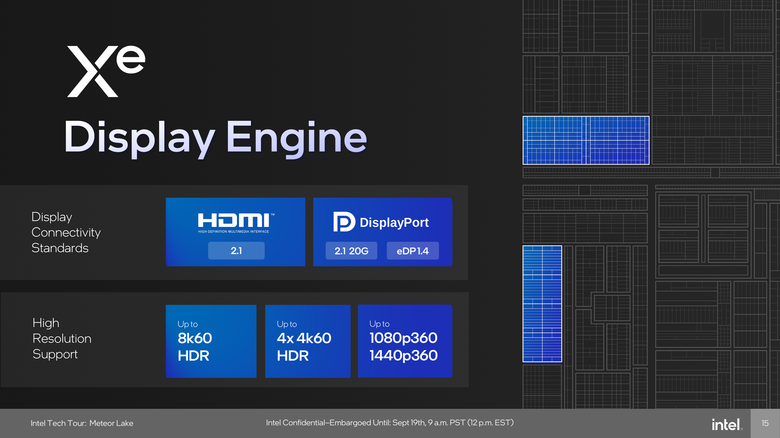
Looking at compatibility, the Xe Display Engine looks to use the latest connections and ports, including native support for HDMI 2.1, DisplayPort 2.1, Embedded DisplayPort (eDP) 1.4. and even DSC 1.2a. Via these blocks, Meteor Lake can support displays up to 8K60 HDR, or up to 4 x 4K60 HDR displays, and this is on top of 1080p360 and 1440p360 too. This gives Meteor Lake substantial display and multimedia device support, including current and up-and-coming panels.


107 Comments
View All Comments
Composite - Thursday, September 28, 2023 - link
totally agree. At the same time, instead of doing a full Intel 4 Meteor lake chip, shrink it down to compute tile only also reduces the size of the silicon and improves yield. Later next year, Intel will also need EUV capacity for Sierra Forest and Granite Rapids. These chips will be much larger than mobile compute tile and considerably lower yield.... Intel will need every ounce of EUV capacity they have.tipoo - Tuesday, September 19, 2023 - link
Probably to have as much compute on the N4 capacity that they have, their substrate also takes much less power connecting them than current AMD and it allows for the best node for each part being used i.e if Intel's wasn't ideal for the GPU tile as the CPU tile etcComposite - Thursday, September 28, 2023 - link
I have the same question. At the same time, I was curious about Intel's EUV capacity. Since Intel is the late comer to EUV and over 50% of EUV machines are at TSMC, does Intel really have the capacity to manufacture full chip Intel 4 Meteor Lake? Not to mention up coming Sierra Forest and later on Granite Rapids will all use EUV capacity. I think the reasonable way is indeed only use EUV at the most critical part of Meteor Lake ---> Compute tile, and out source the rest.eSyr - Tuesday, September 19, 2023 - link
To avoid the issues they have with rollout 14 nm (BDW) and then 10 nm (CNL), I guess, when they held back by yield with respect to particular parts of the chip, specifically, GPU.lemurbutton - Tuesday, September 19, 2023 - link
A17 Pro just beat all Intel CPUs except the 13900KS in ST Geekbench6. A17 Pro uses less than 3w to achieve this - with typical load significantly below 3w. Meanwhile, 13900KS uses as much as 250w or more.Intel's Meteor Lake needs to improve by 10x over Raptor Lake just to match what M3 will be able to do.
Irish_adam - Tuesday, September 19, 2023 - link
The 13900ks uses 250 watts on a single core? Got a link for that?I'll think you find that single core workloads use far, far less. Also remember that benchmarks across ISA's are sketch at best and outright made up at worst. I mean just look how badly games or software can be when ported from one ISA to another, it all really comes down to how well you've made the software to run on each architecture.
Makaveli - Tuesday, September 19, 2023 - link
He is an apple fanboySource: Trust me bro!
FWhitTrampoline - Tuesday, September 19, 2023 - link
No the A17 Performance core is only clocked at 3.6/3.7GHz compared to the x86 designs that are up to clocked 2Ghz+ higher. So this is not some ESPN like Fanatic statement as since the A14/Firestorm core Apple's instruction decoder width is at least 8 decoders wide and backed up by loads of execution ports. And so Apple's P cores are of a very wide order superscalar design since the A14/Firestorm was released!And the Apple P cores are high IPC at low clocks compared to the x86 designs that have 4/6 instruction decoders so need the higher clocks to make up the IPC deficiency for single thread performance that's calculated as IPC multiplied by average sustained clocks to get that single threaded performance metric.
The lower clocks are where Apple's power savings come from and the longer battery life is obtained. That and the A17 Pro/Earlier A series SOCs have loads of specialized heterogeneous compute for offloading workloads onto instead of using the CPU cores or GPU cores so more power can be saved there for all sorts of specialized workloads. The x86 processors/SOCs are just now getting the same sorts of specialized heterogeneous compute IP blocks but that's relatively immature compare to Apple's SOCs and other ARM Based SOC ecosystems that have been using that specialized heterogeneous compute IP for years now.
GeoffreyA - Thursday, September 21, 2023 - link
Well, it would be interesting to see Intel or AMD make a fixed-width ISA design and how that then stacks up against the stuff of Apple. Really, x86 is at a disadvantage because of the variable-width instructions but still has done a fantastic job. Or, I'd like to see Apple design an x86 CPU and see how that holds up against Zen and the rest.FWhitTrampoline - Thursday, September 21, 2023 - link
No logical reason for Apple to go CISC as the x86 Instruction Decoder requires many times the transistors to implement than the transistors required to implement a RISC ISA Instruction Decoder! So it was easy to get 8 Instruction Decoders to fit on the front of the A14/Firestorm processor core(RISC ISA Based). It's easier to go wider if one has a relatively fewer Instructions of a fixed length to implement in a Instruction Decoder design. So that makes it easy to produce a custom very wide order superscalar processor core design that targets high IPC at a lower clock rate and the SOC's CPU cores clocked well inside their Performance/Watt sweet spot. And to still have that A14 match/get close to the x86 cores in single threaded performance and against x86 core designs that are clocked 2GHz+ higher.The x86 ISA is too Legacy Instructions bloated and it's not going to be easy to refactor that and not require years in the process to do that. The ARM ISA ecosystem is from the ground up RISC there and even though the x86 designers have a RISC like back end to break those CISC down into more RISC like instructions, that hardware engine take more transistors to implement and thus will use more power resources getting that done. The vast majority of ARM ISA instructions translate 1 to 1 into single and some a few Micro-OPs so how hard is that to decode compared to x86 ISA instruction that mostly have multiple micro-ops generated to get all that complex work done. And there's a valid power usage reason that x86 never made any inroads into the wider tablet/smartphone market.
The thing about the ARM/RISC core designs is that they can scale from phones to server/HPC whereas the CISC designs can not scale down as low power as RISC designs! but Intel has done a good job at getting close there but a little too late to matter to the OEMs that really did not want to remain beholden to Intel and x86. And the same can be said now for RISC-V compared to an ARM Holdings that's maybe leaning more towards an x86 like business model where RISC-V represents total end user ISA freedom there, within reason, as the RISC-V ISA is totally open not royalist/encumberments required/enforced.