Intel Unveils Meteor Lake Architecture: Intel 4 Heralds the Disaggregated Future of Mobile CPUs
by Gavin Bonshor on September 19, 2023 11:35 AM ESTSoC Tile, Part 1: Low-Power Island E-Cores, Designed for Ultimate Efficiency
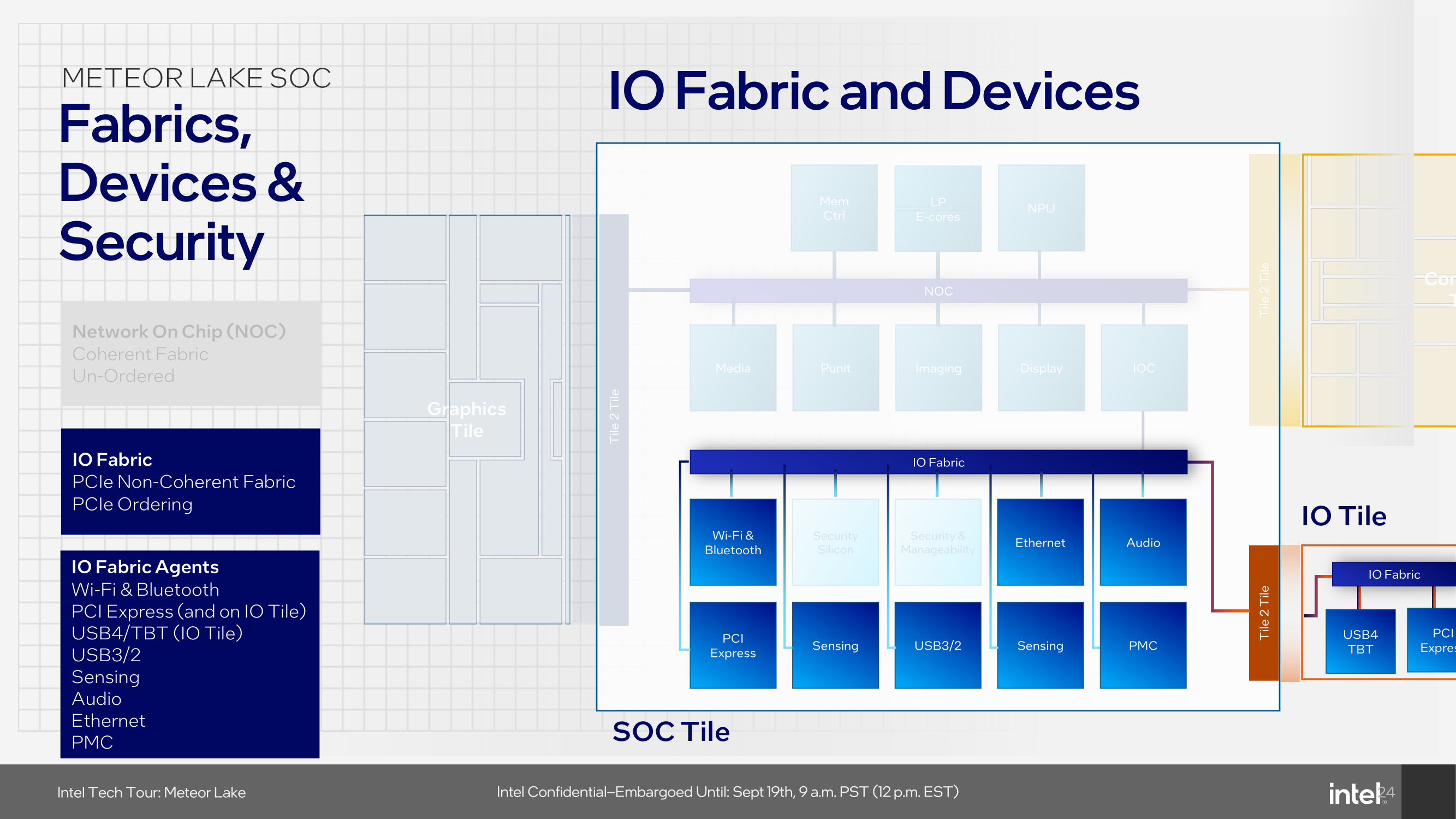
Diving a little deeper into the SoC tile within Intel's Meteor Lake architecture, Intel hasn't just opted for a minor change but has made a significant leap forward, especially regarding I/O fabric scalability. The SoC tile itself isn't built on Intel 4 like the compute tile but is made by TSMC on their N6 node. Intel has ditched the old limitations of mesh routing by implementing a Network-On-Chip (NOC) on the silicon. This isn't just about making data lanes faster; it's about outlining smarter and more power-efficient access to memory. Likely an innovation from Intel's acquisition of NetSpeed back in 2018, which specialized in NoC and Fabric IP for SoCs, Intel opting for a physical NOC allows Intel to reduce the limits on bandwidth. Using EMIB and the nature of 2D scaling, the data paths are a lot shorter, translating into less power loss, but shorter wires also help reduce overall latency penalties.
Switching gears to low-power workload efficiency, Meteor Lake incorporates E-cores directly into the SoC tile, which Intel calls Low Power Island (LP) E-cores. Think of it as Intel's way of saying, "Why use a sledgehammer when a scalpel will do?". This means that the LP E-Cores are driven purely from a power-saving perspective. Having these LP E-cores available for workloads with the aid of Intel's Thread Director means lighter threads and background tasks that don't require the grunt of the P and E-cores on the compute tile can be directed onto the lower-powered LP E-cores.
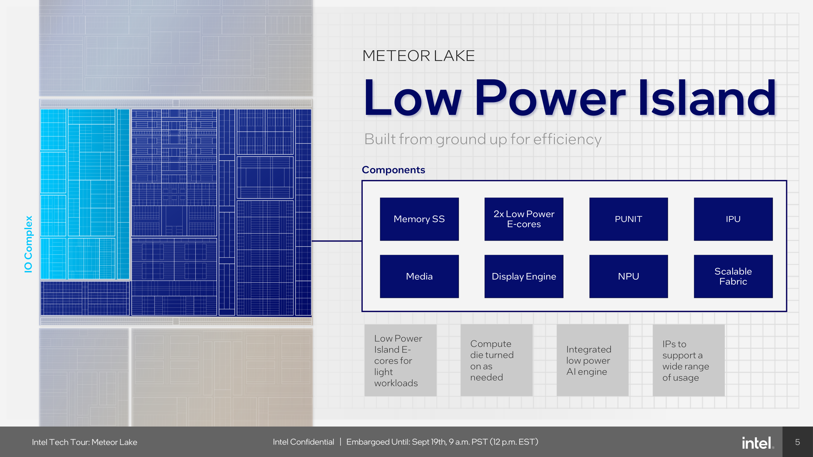
While both the E and LP E-cores are based on the same Crestmont microarchitecture, the E-cores on the compute tile are built on Intel 4, along with the P-cores. The LP E-cores are made on TSMC's N6 node, like the rest of the SoC tile. These low-power island E-cores are tuned for finer-grained voltage control through an integrated Digital Linear Voltage Regulator (DLVR), and they also have a lower voltage-to-frequency (V/F) curve than the big E-cores on the compute tile, meaning they can operate with a lower power cost, thus saving power when transitioning low-intensity workloads off of the compute tile and onto the LP E-cores.
Part of the disaggregated nature of Foveros combined with individual power management controllers (PMC) within each tile means that IP blocks can be independently powered on or off when required.
SoC Tile: Bandwidth Scalability, Can't Stop The NOC
So adding a variety of tiles requires a highly competent pathing to ensure bandwidth is adequately structured. As I/O bandwidth bottlenecking was a major concern in previous iterations, Intel aims to solve bandwidth flow restrictions with a couple of solutions.
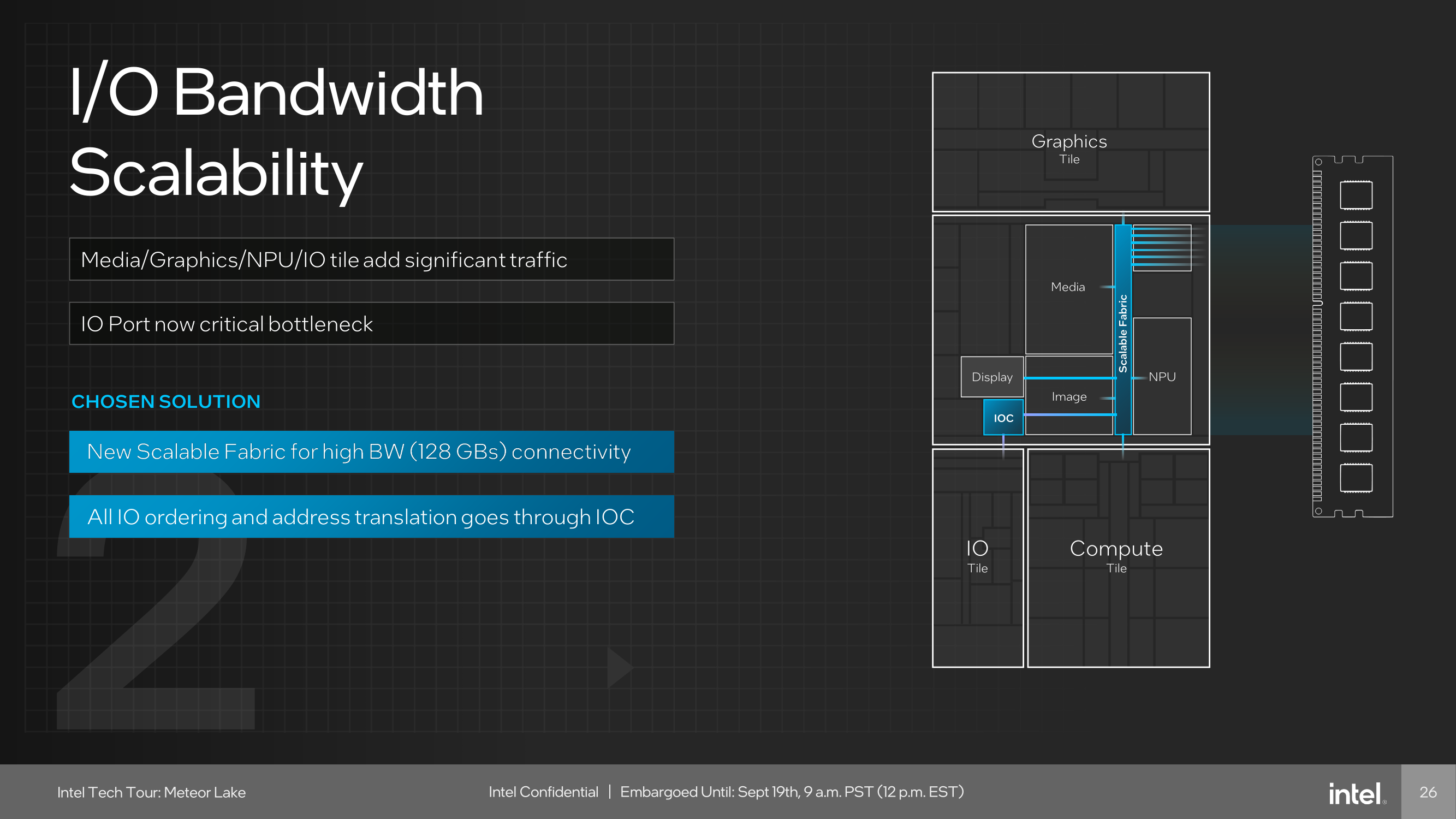
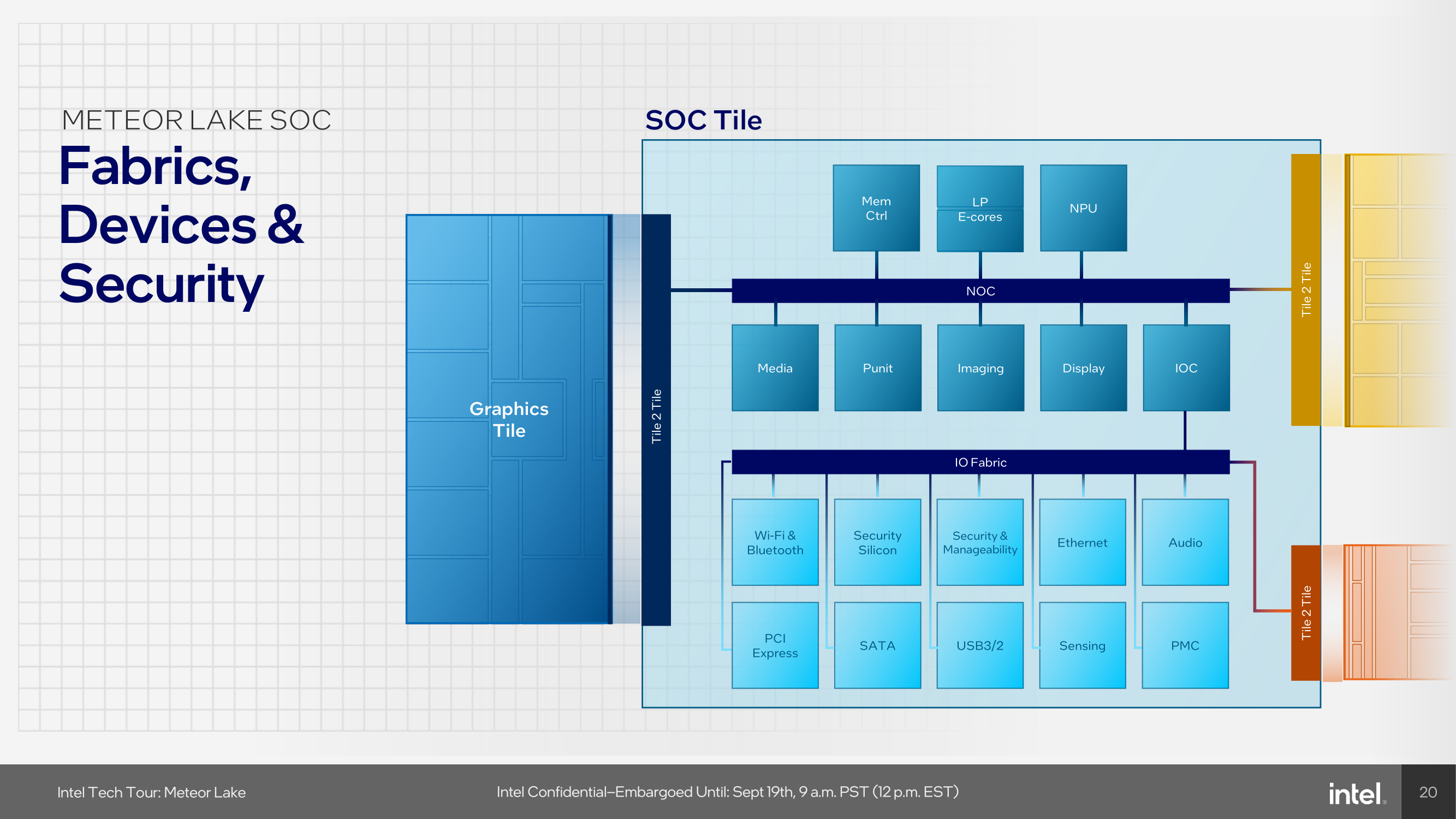
The first is through the scalability of the I/O bandwidth, which Intel does by adding what it calls 'Scalable Fabric,' which is configured for up to 128 GB/s of bandwidth throughput. All of the I/O ordering and address translation is fed through the IOC, while Intel has implanted a Network-on-Chip (NOC) to interconnect many of the different areas of the SoC.
The Network-on-Chip or NOC is designed to be coherent, and for Meteor Lake on Intel 4, this uses unordered processing, which moves data in an unordered fashion. Connecting all the tiles together through the NOC and independently through the IOC gives plenty of bandwidth headroom for devices or agents requiring it. The NOC is directly connected to the compute and graphics tile, while other elements, including the traffic fed directly through the LP E-cores on the SoC tile, media, display, the NPU, and the imaging processing unit (IPU), all going through the NOC. In terms of the connection to the I/O tile, this is connected directly to the IO fabric and then is fed through the IOC, which then goes directly to the NOC.
The SoC tile also integrates Wi-Fi 6E and can be made to support the latest Wi-Fi 7 standard. Having a future-proof method of including Wi-Fi 7 and Bluetooth 5.4 can add the next level of wireless connectivity to Intel's mobile platform. Wi-Fi 7 offers 320 MHz of bandwidth, doubling the channel width compared to its predecessor, Wi-Fi 6. It also uses 4096-QAM (4K QAM) to enable transmission speeds capable of hitting 5.8 Gbps.
We're still waiting for clarification on what this actually means. Whether it's supportive of Wi-Fi 7 or if there's some underlying compatibility within the Wi-Fi MAC integrated into the silicon. One option could be that Intel is adding a full external controller into the silicon to get to Wi-Fi 7 instead of CNVio splitting up parts of the radio stack. We have asked Intel for more details and will update you when we have a response.
That being said, Intel discloses 'support' for Wi-Fi 7 and BT 5.4, but there's a chance Intel could differentiate which wireless MAC is implemented into different chip segments. An example would be an Intel 9 Ultra SKU, bolstered by Wi-Fi 7 support, whereas a lower-end SKU like a Core 3 might utilize Wi-Fi 6E to save on cost.
Additional features include Multi-Resource Unit (RU) Puncturing and Military-grade security with WPA3 that supports GCMP-256 encryption to ensure both speed and security when connected to a wireless network. Unique features like Multi-Link Operation (MLO) in Wi-Fi 7 are designed to reduce latency and jitter by up to 60%, making it a competent solution for various user's connectivity needs. Adding Bluetooth 5.4 further complements this by improving audio quality, and it is claimed to offer up to 50% lower power consumption for longer battery life.
Also present on the SoC tile is the display controller and the media engine from the GPU. These are always-on (or at least, mostly-on) blocks that do not need to be built on a cutting-edge process node, making them good candidates to place on the SoC tile. Meteor Lake offers support for 8K HDR and AV1 video playback and contains native HDMI 2.1 and DisplayPort 2.1 connectivity.
Finally, the SoC tile also includes other key platform components, such as PCIe lanes, which are integral for connectivity to external devices such as discrete graphics cards and the platform's I/O capabilities, such as USB 4 and 3, as well as offering a direct interconnect to a separate I/O tile with Thunderbolt 4 and additional PCIe lanes. While we've touched on wireless connectivity, the SoC tiler also includes Ethernet support, although Intel hasn't disclosed yet which PHY will be included; it is likely to be capable of 2.5 GbE at the minimum.
A Note on Meteor Lake's Security Features: New Silicon Security Engine (ISSE)
Security has also been given closer attention in Meteor Lake. The architecture introduces the Intel Silicon Security Engine (ISSE), a dedicated component focused solely on securing things at a silicon level. Various vulnerabilities have been at the forefront of media over the last few years, including Meltdown, Spectre, and Foreshadow.
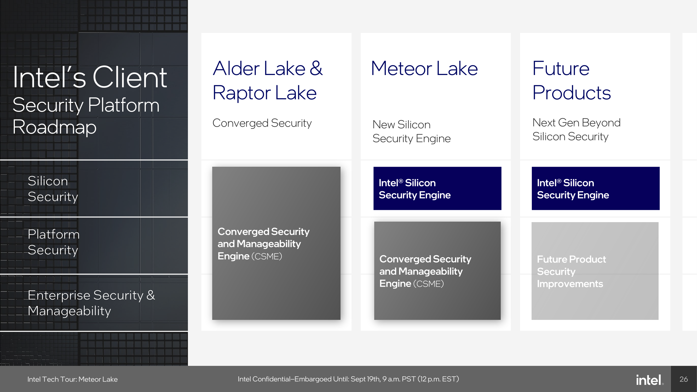
With real threats around the world, securing data is ever prevalent, and CPU architects and designers not only need to consider performance and efficiency, but security and doing some architecturally is just as important as a competent software stack. The Converged Security and Manageability Engine (CSME) has also been partitioned to further enhance platform security. These features collectively work to give a wide range of on-chip and off-chip securities designed to mitigate attacks on multiple fronts.


107 Comments
View All Comments
Composite - Thursday, September 28, 2023 - link
totally agree. At the same time, instead of doing a full Intel 4 Meteor lake chip, shrink it down to compute tile only also reduces the size of the silicon and improves yield. Later next year, Intel will also need EUV capacity for Sierra Forest and Granite Rapids. These chips will be much larger than mobile compute tile and considerably lower yield.... Intel will need every ounce of EUV capacity they have.tipoo - Tuesday, September 19, 2023 - link
Probably to have as much compute on the N4 capacity that they have, their substrate also takes much less power connecting them than current AMD and it allows for the best node for each part being used i.e if Intel's wasn't ideal for the GPU tile as the CPU tile etcComposite - Thursday, September 28, 2023 - link
I have the same question. At the same time, I was curious about Intel's EUV capacity. Since Intel is the late comer to EUV and over 50% of EUV machines are at TSMC, does Intel really have the capacity to manufacture full chip Intel 4 Meteor Lake? Not to mention up coming Sierra Forest and later on Granite Rapids will all use EUV capacity. I think the reasonable way is indeed only use EUV at the most critical part of Meteor Lake ---> Compute tile, and out source the rest.eSyr - Tuesday, September 19, 2023 - link
To avoid the issues they have with rollout 14 nm (BDW) and then 10 nm (CNL), I guess, when they held back by yield with respect to particular parts of the chip, specifically, GPU.lemurbutton - Tuesday, September 19, 2023 - link
A17 Pro just beat all Intel CPUs except the 13900KS in ST Geekbench6. A17 Pro uses less than 3w to achieve this - with typical load significantly below 3w. Meanwhile, 13900KS uses as much as 250w or more.Intel's Meteor Lake needs to improve by 10x over Raptor Lake just to match what M3 will be able to do.
Irish_adam - Tuesday, September 19, 2023 - link
The 13900ks uses 250 watts on a single core? Got a link for that?I'll think you find that single core workloads use far, far less. Also remember that benchmarks across ISA's are sketch at best and outright made up at worst. I mean just look how badly games or software can be when ported from one ISA to another, it all really comes down to how well you've made the software to run on each architecture.
Makaveli - Tuesday, September 19, 2023 - link
He is an apple fanboySource: Trust me bro!
FWhitTrampoline - Tuesday, September 19, 2023 - link
No the A17 Performance core is only clocked at 3.6/3.7GHz compared to the x86 designs that are up to clocked 2Ghz+ higher. So this is not some ESPN like Fanatic statement as since the A14/Firestorm core Apple's instruction decoder width is at least 8 decoders wide and backed up by loads of execution ports. And so Apple's P cores are of a very wide order superscalar design since the A14/Firestorm was released!And the Apple P cores are high IPC at low clocks compared to the x86 designs that have 4/6 instruction decoders so need the higher clocks to make up the IPC deficiency for single thread performance that's calculated as IPC multiplied by average sustained clocks to get that single threaded performance metric.
The lower clocks are where Apple's power savings come from and the longer battery life is obtained. That and the A17 Pro/Earlier A series SOCs have loads of specialized heterogeneous compute for offloading workloads onto instead of using the CPU cores or GPU cores so more power can be saved there for all sorts of specialized workloads. The x86 processors/SOCs are just now getting the same sorts of specialized heterogeneous compute IP blocks but that's relatively immature compare to Apple's SOCs and other ARM Based SOC ecosystems that have been using that specialized heterogeneous compute IP for years now.
GeoffreyA - Thursday, September 21, 2023 - link
Well, it would be interesting to see Intel or AMD make a fixed-width ISA design and how that then stacks up against the stuff of Apple. Really, x86 is at a disadvantage because of the variable-width instructions but still has done a fantastic job. Or, I'd like to see Apple design an x86 CPU and see how that holds up against Zen and the rest.FWhitTrampoline - Thursday, September 21, 2023 - link
No logical reason for Apple to go CISC as the x86 Instruction Decoder requires many times the transistors to implement than the transistors required to implement a RISC ISA Instruction Decoder! So it was easy to get 8 Instruction Decoders to fit on the front of the A14/Firestorm processor core(RISC ISA Based). It's easier to go wider if one has a relatively fewer Instructions of a fixed length to implement in a Instruction Decoder design. So that makes it easy to produce a custom very wide order superscalar processor core design that targets high IPC at a lower clock rate and the SOC's CPU cores clocked well inside their Performance/Watt sweet spot. And to still have that A14 match/get close to the x86 cores in single threaded performance and against x86 core designs that are clocked 2GHz+ higher.The x86 ISA is too Legacy Instructions bloated and it's not going to be easy to refactor that and not require years in the process to do that. The ARM ISA ecosystem is from the ground up RISC there and even though the x86 designers have a RISC like back end to break those CISC down into more RISC like instructions, that hardware engine take more transistors to implement and thus will use more power resources getting that done. The vast majority of ARM ISA instructions translate 1 to 1 into single and some a few Micro-OPs so how hard is that to decode compared to x86 ISA instruction that mostly have multiple micro-ops generated to get all that complex work done. And there's a valid power usage reason that x86 never made any inroads into the wider tablet/smartphone market.
The thing about the ARM/RISC core designs is that they can scale from phones to server/HPC whereas the CISC designs can not scale down as low power as RISC designs! but Intel has done a good job at getting close there but a little too late to matter to the OEMs that really did not want to remain beholden to Intel and x86. And the same can be said now for RISC-V compared to an ARM Holdings that's maybe leaning more towards an x86 like business model where RISC-V represents total end user ISA freedom there, within reason, as the RISC-V ISA is totally open not royalist/encumberments required/enforced.