AMD's Fab 36 Grand Opening - 90nm and 300mm in Germany
by Anand Lal Shimpi on October 14, 2005 7:50 AM EST- Posted in
- CPUs
After 24 months of construction, today AMD's first 300mm semiconductor fab, Fab 36, celebrates its grand opening. Built adjacent to AMD's 200mm Fab 30 in Dresden, Germany, Fab 36's grand opening takes place 6 years after Fab 30's introduction. The name Fab 36 comes from its existence 36 years after the founding of AMD.
The announcement for Fab 36's site in Dresden came in November 2003, with first ground breaking at the end of that month. Approximately 12 months later, the building was ready for equipment, and another 12 months after that, Fab 36 began preparations for mass production.
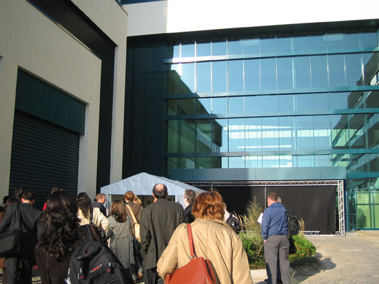
Over 150 members of the press enter AMD's press conference at Fab 36 in Dresden
Unfortunately, at its grand opening, Fab 36 is still a 90nm-only fab; throughout the next year, AMD will begin the transition to 65nm production. The first CPUs built at Fab 36 will be shipping in the first quarter of 2006, with the first 65nm chips leaving Fab 36 by the end of 2006.
Sometime in 2007 AMD will have performed a "substantial amount" of the transition of Fab 36 to a 65nm semiconductor fab, bringing the grand total for the cost of Fab 36 to an astounding 2.5 billion US dollars. There is no word when Fab 36 will be completely converted to 65nm manufacturing.
By 2008, Fab 36 will be able to produce more than 2x the number of processors as Fab 30 (potentially 100M processors per year based on current die sizes).
The first 300mm wafer produced at Fab 36 actually took place back in March, but preparation for mass production continues up to and beyond today. Today's grand opening of Fab 36 marks a huge step in AMD history, as it will hopefully alleviate a number of the supply issues they have been plagued with in recent history.
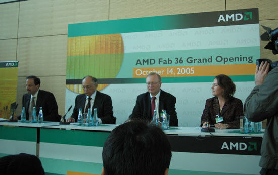
The two individuals in the middle kicked off the day at Fab 36, AMD's CEO, Dr. Hector Ruiz is the second on the left, and VP/GM of AMD Dresden, Dr. Hans Deppe is to the right of Dr. Ruiz.
The day started off with a press conference kicking off the grand opening of the fab. Below we've got a picture of a clean room engineer (or someone dressed as one) posing with AMD's Dr. Hans Deppe, the Corporate VP and General Manager of AMD in Dresden.
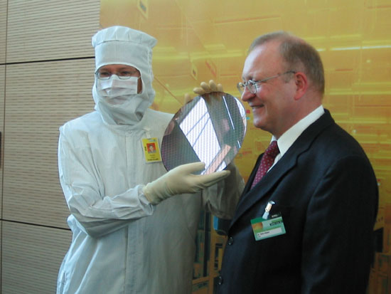
While we don't have a 200mm wafer here to compare sizes with, imagine the wafer pictured above, but smaller.
After some brief words about the opening of Fab 36, a brief Q&A period started. One of the first questions was what will happen to Fab 30 in the future now that Fab 36 is ready to start mass production. Dr. Ruiz mentioned that Fab 30 could be used for more x86 microprocessor production, it could potentially become a chipset manufacturing fab (possibly indicating AMD's intentions to eventually return to chipset manufacturing), or it could be upgraded to future semiconductor technologies for use in the future (e.g. 65nm).
One other important question that was asked was "why Dresden" for Fab 36, to which the answer was obviously multi-faceted:
1) First and foremost, AMD has invested a lot in the people of Dresden, when it comes to training and expertise in semiconductor manufacturing. It was simply easier to leverage the existing human investment.
2) Obviously government subsidies played a large role in AMD's decision to bring Fab 36 to Dresden. Dr. Hans Deppe listed the total amount of government subsidies for Fab 36 as 500 million US dollars.
The final question of the press conference was about AMD's future fab plans, which Dr. Ruiz answered with a timeframe of 2008 for the start of production on the next major fab plant.


70 Comments
View All Comments
eljefe2 - Friday, October 14, 2005 - link
I rather it be in a place where they pay real wages. at least it then stops some trends in big business.And yes prior to amd k6-II, amd made some bad things. Then the k6-III, the athlon, xp, a64, dual core, all trumped intel crap. it took me a many years before I realized this.
I think that has been a while now. xp onward has obviously beat out intel for home use, and now, in every use (besides vector graphics, and of course, we all are manipulating vector graphic intensive programs as we type.... yea....)
the only saving thing is pentium M for intel. and they have refused to release that as a desktop chip for many years. how crappy can you get. I just want to know WHY people are so supportive of a poorly serving the public company which HAD the means to provide much better products than AMD yet refused to.
eljefe2 - Friday, October 14, 2005 - link
.... i meant i rather it be in a place that gives real wages, either US or in Europe, other than some random asian country.nserra - Friday, October 14, 2005 - link
Remember that AMD processors are not made of the same "compounds" of Intel processors.Maybe AMD could also launch a 65nm based processor based on "compounds" of Intel processors.
As
Intel could "never" launch NOW a 65nm based processor using AMD "compounds".
eljefe2 - Friday, October 14, 2005 - link
15-18% difference in wattage pull at max draw and no difference in performance is what intel got out of 65nm process.THAT's IT.
at that level, amd still blows it away at 90 nm. amd hasnt moved to 65nm because it is not a crappy chip company. it always does better than the other companies at the larger nm size. Why should it have to change? when it does, it will be even better, which will be fantastic, not just an inflated figure. Idle wattages are most important and so intel hasnt anything to say about that at all still with their 65nm process. (chips dont go full max all that often in the real world, and when they do, the 65nm intels are still power hogs.)
Shintai - Saturday, October 15, 2005 - link
You mean 65nm suck like:Dothan -> Yonah: 1 extra core, better FPU, better SSE, higher FSB and better cache for 4W extra (31W total) aswell as cheaper to make than a single Dothan? (A dual Dothan with 667FSB would use about 60-65W)
Prescott -> Cedar Mill(?): 15/25W drop in powerusage and 25-30% cheaper to manuafacture?
Smithfield -> "Whatever the dualcore is named": Same as above, just with a higher wattage drop.
Ye that kinda seem to suck really bad...
If you think AMD or Intel will boost speedgrades alot with 65nm you gonna be so wrong. It will be more cores, cheaper cores and less power as primary focus.
65nm is just giving Intel a better price/volume advantage the next 12 months.
Spoonbender - Friday, October 14, 2005 - link
haha, that's funny. We need more fanboys who don't know what they're talking about.First, AMD has made some lousy processors in the past, far crappier than anything Intel could ever dream of.
Second, the main reason for advancing to 65nm is not performance, it's cost.
AMD could certainly benefit from doubling the number of dies per wafer. Even if they OMFGR0XXORZ Intel's chips performance-wise.
Griswold - Friday, October 14, 2005 - link
Spoken like a true fanboi.
trooper11 - Friday, October 14, 2005 - link
but the point is it wont kill amd if they dont have 65nm parts out to market will the 2nd half of 06Spoonbender - Friday, October 14, 2005 - link
Well, it will prevent them from lowering prices as much as Intel can do without actually losing money. Of course, that probably won't *kill* them, but it can hurt them. They only recently got into the habit of making a profit at all. Having their production costs around twice Intel's level is bad. (Although admittedly, I believe the P4 dies are way bigger than A64's, so they do partially compensate there)coldpower27 - Friday, October 14, 2005 - link
Don't use NetBurst as a yardstick for the 65nm process, think of it this way, if the 65nm process can reduce heat disppation for NetBurst technology, think of what it could for Pentium M based technology or Merom/Conroe.Remember heat disppation was reduced on the Banias to Dothan Pentium M transition and that core still uses the same 90nm process as Prescott did.