The Intel 12th Gen Core i9-12900K Review: Hybrid Performance Brings Hybrid Complexity
by Dr. Ian Cutress & Andrei Frumusanu on November 4, 2021 9:00 AM ESTCPU Tests: Core-to-Core and Cache Latency, DDR4 vs DDR5
Starting off with the first of our synthetic tests, we’re looking into the memory subsystem of Alder Lake-S, as Intel has now included a great deal of changes to the microarchitecture, both on a chip-level, as well as on a platform-level due to the new DDR5 memory compatibility.
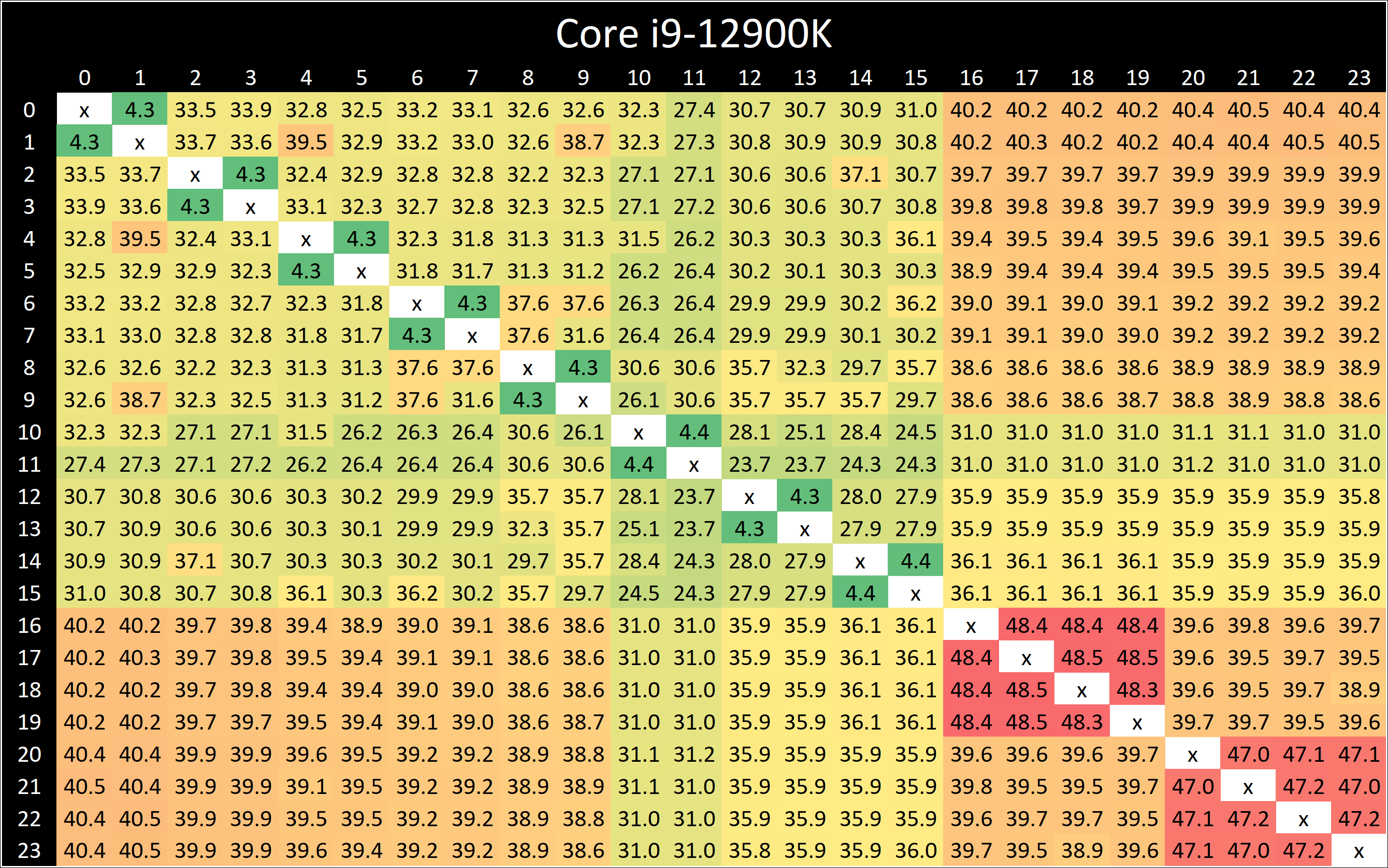
In our core-to-core latency test which showcases the physical topology of the chip, there’s a few things to note. Beginning with the P-cores, which are logically enumerated in the operating system as cores 0 to 15, we can see that latencies are about the same as what we’ve seen on Rocket Lake, although with a few nanosecond differences in the results. The latencies appear to be a bit more topologically uniform, which might indicate that Intel might have finally gotten rid of their uni-directional coherency snoop ring for a bi-directional one.
Latencies between the SMT siblings are also interesting as they decrease from 5.2ns on the Willow Cove cores to 4.3ns on the new Golden Cove cores. The actual L1 access latencies haven’t changed between the two microarchitectures, which means that Intel has improved the LOCK instruction cycle latency.
Between the Golden Cove cores and the smaller Gracemont cores we see higher latencies, as that was to be expected given their lower clock speeds and possible higher L2 overhead of the Gracemont cluster.
What’s however a bit perplexing is that the core-to-core latencies between Gracemont cores is extremely slow, and that’s quite unintuitive as one would have expected coherency between them to be isolated purely on their local L2 cluster. Instead, what seems to be happening is that even between two cores in a cluster, requests have to travel out to the L3 ring, and come back to the very same pathway. That’s quite weird, and we don’t have a good explanation as to why Intel would do this.
Cache Latencies and DDR5 vs DDR4
Next up, let’s take a look at the new cache hierarchy of Alder Lake, both from the view of the Golden Cove cores as well as the Gracemont cores, in DDR5 as well as DDR4.
Alder Lake changes up the big cores cache quite considerably. First off, the L1D remains identical – so not much to report there.
On the L2 side of things, compared to Rocket Lake’s Willow Cove cores, Alder Lake’s Golden Cove cores considerably increase the L2 cache from 512KB to 1.25MB. This does come at a 15% latency degradation for this cache, however given the 2.5x increase in size and thus higher hit rates, it’s a good compromise to make.
The Gracemont E-cores have a large 2MB L2 which is shared amongst the 4 cores in a cluster, so things do look quite differently in terms of hierarchy. Here latencies after 192KB do increase for some patterns as it exceeds the 48-page L1 TLB of the cores. Same thing happens at 8MB as the 1024-page L2 TLB is exceeded.
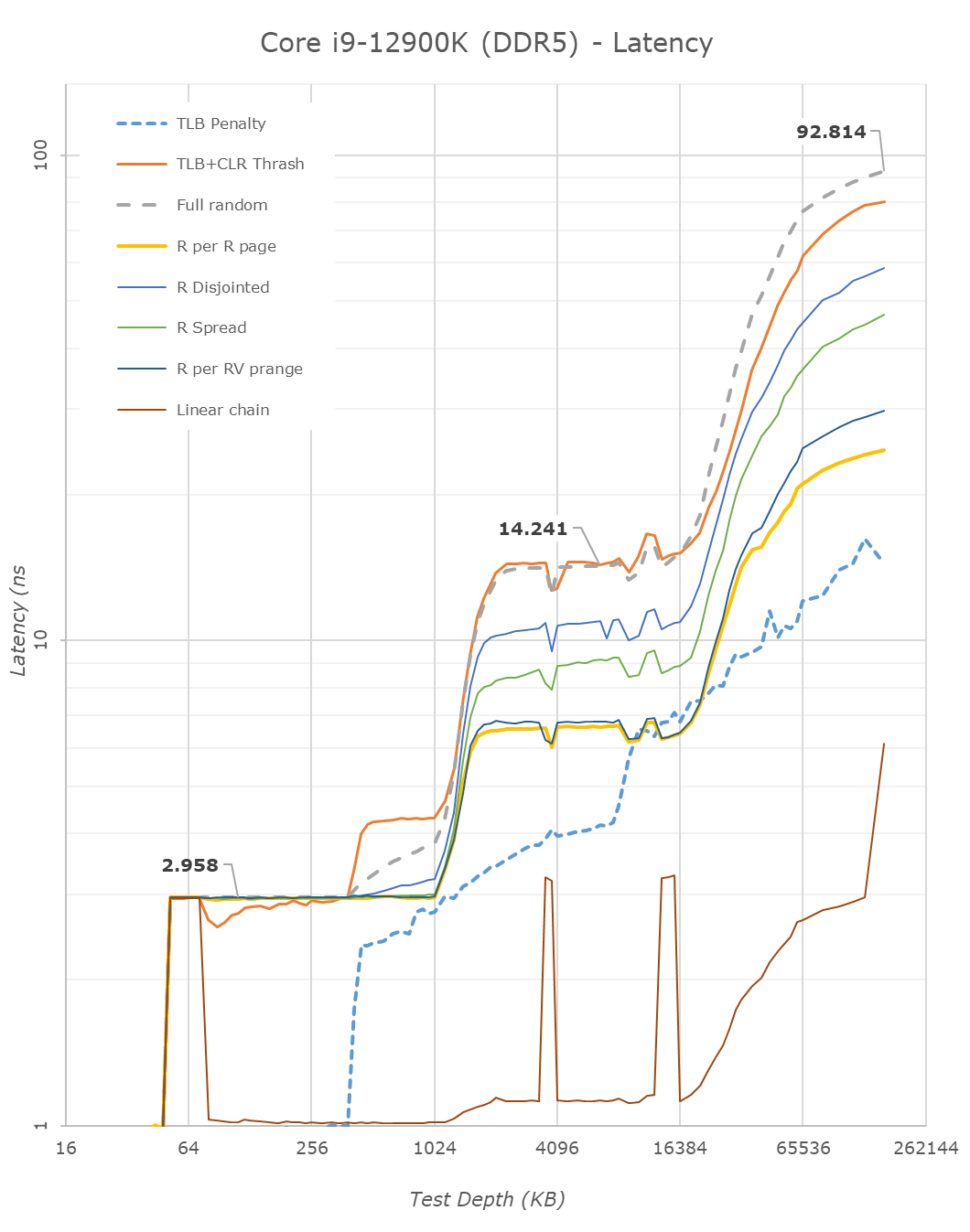
The L3 cache of the chip increases vastly from 16MB in RKL to 30MB in ADL. This increase also does come with a latency increase – at equal test depth, up from 11.59ns to 14.24ns. Intel’s ring and cache slice approach remains considerably slower than AMD’s CCX, which at a similar L3 size of 32MB comes in at 10.34ns for equivalent random-access patterns.
On the DRAM side of things, we can start off with the RKL DDR4 to ADL DDR4 results. The memory latency at 160MB goes up from 85ns to 90ns – generally expected given the larger memory subsystem of the new chip.
Shifting over from DDR4 to the DDR5 results on Alder Lake, at JEDEC speeds, comparing DDR4-3200 CL20 to DDR4-4800 CL40, the officially supported speeds of the chip, we see memory latency only go up to 92.8ns, which is actually below our expectations. In other prefetcher-friendly patterns, latency goes up by a larger 5ns, but still that’s all within reasonable figures, and means that DDR5 latency regressions we feared are overblown, and the chip is able to take advantage of the new memory type without any larger issues.
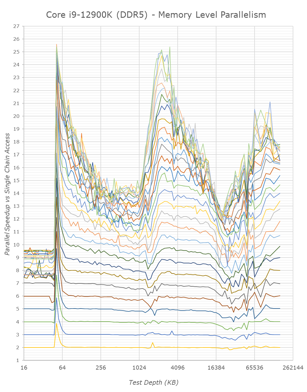
We only ever whip out our memory level parallelism test when there’s a brand-new microarchitecture which changes things quite considerably in regards to how it handles MLP. Alder Lake and its Golden Cove and Gracemont cores are such designs.
Memory level parallelism is the characteristic of a CPU being able to have multiple pending memory accesses – instead of doing things serially, out of order CPUs are able to fetch data from multiple memory locations at the same time. The definition of how many accesses this ends up as, depends on the design within the core, such as MHSR’s, but also the actual parallelism of the various caches as well as the fabric itself. Our test here compares the relative speedup of doing parallel access of random pointer chain chasing – a speedup of 2x means that the core is able to access two chains simultaneously with no degradation of per-element access times. At some point, we’ll be hitting bottlenecks of the various memory elements of the core and memory subsystem. A higher MLP speedup allows for faster execution in workloads which have data-level parallelism, and also improves the ability to hide latency in terms of performance.
Intel’s Golden Cove core is here a massive uplift in terms of its MLP capabilities. The L2 cache of the chip, because it’s so much larger, likely also has a lot more physical banks to it, likely allowing more parallel accesses.
On the L3 cache, Intel also notably mentioned that the new design is able to handle more outstanding transfers, as we immediately see this in the results of Golden Cove. Our test here only tracked up to 30 parallel accesses and we didn’t have time to check out a more extended test, but it does seem the core would be able to hit higher figures – at least until it hits TLB limits, where things slow down. The MLP capabilities here are similar, if not greater, than what AMD showcases in their Zen CPUs, something we had noted as being a strength of their microarchitecture.
MLP at deeper DRAM regions is essentially double that of Rocket Lake – at least on the DDR5 variant of Alder Lake. The DDR4 results reduce the MLP advantage, likely because the chip has to deal with only 2 memory channels rather than 4 on the DDR5 test, this allows the DDR5 variant more parallel sparse accesses to DRAM banks. Interestingly, Intel still doesn’t do as well as AMD even with DDR5 – I’m not sure where exactly the differences stem from, but it must be further down the fabric and memory controller side of things.
From the E-core Gracemont cores, the results also look good, albeit the L3 parallelism looks lower – maybe that’s a limit of the outstanding requests from the L2 cluster of the GRM cores – or maybe some interface limitation.
I think the MLP improvements of Alder Lake here are extremely massive, and represent a major jump in terms of memory performance of the design, something which undoubtedly lead to larger IPC gains for the new microarchitecture.


474 Comments
View All Comments
Kvaern1 - Sunday, November 7, 2021 - link
Because there are no games which are 'incompatible'' with ADL.eastcoast_pete - Sunday, November 7, 2021 - link
While AL is an interesting CPU (regardless of what one's preference is), I still think the star of AL is the Gracemont core (E cores), and did some very simple-minded, back of a napkin calculations. The top AL has 8 (P cores with multithreading) = 16 + 8 E core threads (no multithreading here) for a total of 24 threads. According to first die shots, one P core requires the same die area as 4 E cores. That leaves me wanting an all-E core CPU with the same die size as the i9 AL, because that could fit 8x4= 32 plus the existing 8 Gracemonts, for a total of 40. And, the old problem of "Atoms can't do AVX and AVX2" is solved - because now they can! Yes, single thread performance would be significantly lower, but any workload that can take advantage of many threads should be at least as fast as on the i9. Anyone here knows if Intel is considering that? It wouldn't be the choice for gaming, but for productivity, it might give both the i9 and, possibly, the 5950x a run for the money.mode_13h - Monday, November 8, 2021 - link
They currently make Atom-branded embedded server CPUs with up to 24 cores. This one launched last year, using Tremont cores:https://ark.intel.com/content/www/us/en/ark/produc...
I think you can expect to see a Gracemont-based refresh, possibly with some new product lines expanding into non-embedded markets.
eastcoast_pete - Monday, November 8, 2021 - link
Yes, those Tremont-based CPUs are intended/sold for 5G cell stations; I hope that Intel doesn't just refresh those with Gracemont, but makes a 32-40 Gracemont core CPU available for workstations and servers. The one thing that might prevent that is fear (Intel's) of cannibalizing their Sapphire Rapid sales. However, if I would be in their shoes, I'd worry more about upcoming AMD and multi-core ARM server chips, and sell all the CPUs they can.mode_13h - Tuesday, November 9, 2021 - link
Well, it's a start that Intel is already using these cores in *some* kind of server CPU, no? That suggests they already should have some server-grade RAS features built-in. So, it should be a fairly small step to use them in a high core count CPU to counter the Gravitons and Altras. I think they will, since it should be more competitive in terms of perf/W.As for workstations, I think you'll need to find a workstation board with a server CPU socket. I doubt they'll be pushing massive E-core -only CPUs specifically for workstations, since workstation users also tend to care about single-thread performance.
anemusek - Sunday, November 7, 2021 - link
Sorry but performance it isn't all +- a few percent in the real world will not restore confidence. Critical flaws, disabling functionality (dx12 in hanswell for example), instabbility instruction features etc.I cannot afford to trust such a company
Dolda2000 - Sunday, November 7, 2021 - link
I just wanted to add a big Kudos for this article. AnandTech's coverage of the 12900K was by a wide margin the best of any I read or watched, with regards to coverage of the various variables involved, and with the breadth and depth of testing. Thanks for keeping it up!chantzeleong - Monday, November 8, 2021 - link
I run Power bi and tensorflow with large dataset. Which Intel CPU do you recommend and why?mode_13h - Tuesday, November 9, 2021 - link
I don't know about "Power bi", but Tensorflow should run best on GPUs. Which CPU to get then depends on how many GPUs you're going to use. If >= 3, then Threadripper. Otherwise, go for Alder Lake or Ryzen 5000 series.You'll probably find the best advice among user communities for those specific apps.
velanapontinha - Monday, November 8, 2021 - link
We've seen this before. It is time to short AMD, unfortunately.