The Intel 12th Gen Core i9-12900K Review: Hybrid Performance Brings Hybrid Complexity
by Dr. Ian Cutress & Andrei Frumusanu on November 4, 2021 9:00 AM ESTCPU Tests: SPEC MT Performance - DDR5 Advantage
Multi-threaded performance is where things become very interesting for Alder Lake, where the chip can now combine its 8 P-cores with its 8 E-cores. As we saw, the 8 E-cores are nothing to sneeze about, but another larger consideration for MT performance is DDR5. While in the ST results we didn’t see much change in the performance of the cores, in MT scenarios when all cores are hammering the memory, having double the memory channels as well as +50% more bandwidth is going to be extremely beneficial for Alder Lake.
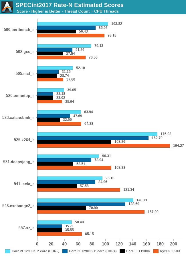
As we noted, the DDR5 vs DDR4 results showcase a very large performance gap between the two memory technologies in MT scenarios. Running a total of 24 threads, 16 for the SMT-enabled P-cores, and 8 for the E-cores, Alder Lake is able to take the performance crown in quite a lot of the workloads. There are still cases where AMD’s 16-core setup with larger cores are able to perform better, undoubtedly also partly attributed to 64MB of on-chip cache.
Compared to the 11900K, the new 12900K showcases giant leaps, especially when paired with DDR5.
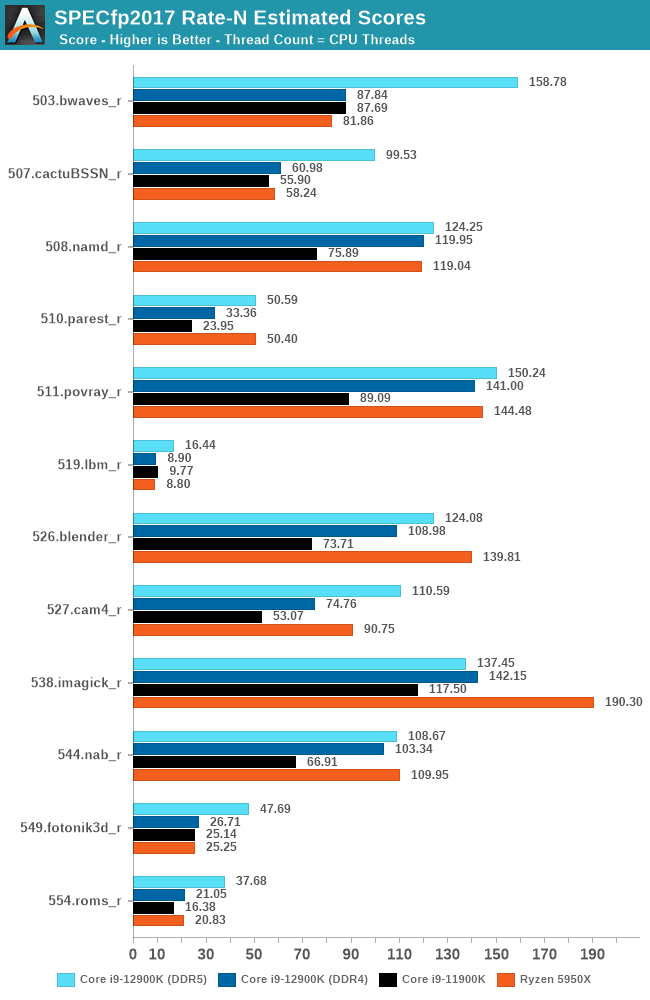
In the FP suite, the DDR5 advantage in some workloads is even larger, as the results scale beyond that of the pure theoretical +50% bandwidth improvement. What’s important for performance is not just the theoretical bandwidth, but the actual utilised bandwidth, and again, the doubled up memory channels of DDR5 here are seemingly contributing to extremely large increases, if the workload can take advantage of it.
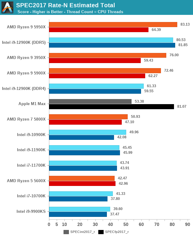
In the aggregate results, there’s very clearly two conclusions, depending on whether you use the chip with DDR5 or DDR4.
With DDR4, Alder Lake and the 12900K in particular, is able to showcase very good and solid increases in performance, thanks to the IPC gains on the Golden Cove core, but most importantly, also thanks to the extra 8 Gracemont cores, which do carry their own weight. The 12900K falls behind AMD’s 5900X with DDR4, which is fair given the pricing of the chips here are generally in line with teach other.
With DDR5, the 12900K is able to fully stretch its multi-threaded performance legs. In less memory dependent workloads, the chip battles it out with AMD’s 16-core 5950X, winning some workloads, losing some others. In more memory dependent workloads, the DDR5 advantage is extremely clear, and the 12900K is able to blow past any competition, even slightly edging out the latest Apple M1 Max, released a few weeks ago, and notable for its memory bandwidth.


474 Comments
View All Comments
mode_13h - Sunday, November 7, 2021 - link
I'm not even going to say this is a bad idea. The problem is that it's a big change and Intel normally prepares the software developer community for big new ISA extensions a year+ in advance!Again, what you're talking about is an ABI change, which is a big deal. Not only that, but to require code to handle dynamically switching between AVX2 and AVX-512 paths means that it can't use different datastructures for each codepath. It even breaks the task pre-emption model, since there need to be some limitations on where the code needs to have all its 512-bit registers flushed so it can handle switching to the AVX2 codepath (or vice versa).
This adds a lot of complexity to the software, and places a greater testing burden on software developers. All for (so far) one CPU. It just seems a bit much, and I'm sure a lot of software companies would just decide not to touch AVX-512 until things settle down.
GeoffreyA - Sunday, November 7, 2021 - link
My view on this topic is that Intel made a sound decision disabling AVX512. Some of the comments are framing it as if they made a mistake, because the tech community discovered it was still there, but I don't see any problem. Only, the wording was at fault, this controversial "fused off" statement. And actually, the board makers are at fault, too, enabling a hidden feature and causing more confusion.On the question of whether it's desirable, allowing one core with the instructions and another without, would've been a recipe for disaster---and that, too, for heaven knows what gain. The simplest approach was bringing both cores onto the same footing. Indeed, I think this whole P/E paradigm is worthless, adding complexity for minimal gain.
Oxford Guy - Monday, November 8, 2021 - link
‘Intel made a sound decision disabling AVX512’That’s not what happened.
O-o-o-O - Sunday, November 7, 2021 - link
Really? Our tech guys tried out Xeon Phi but couldn't make use of it. Years later, Xeon Phi was abruptly discontinued due to lack of demand. GPGPUs are much easier to handle.Yeah, coding cost and risks aside, it's interesting to see complex work of art in the modern CPU. But I'd rather wish for expansion of GPU support (like shared memory and higher band-width).
kwohlt - Sunday, November 7, 2021 - link
My understanding is that Raptor Lake's change is replacing Golden Cover P cores with Raptor Cove P cores, doubling Gracemont E-Cores per SKU, and using the same Intel 7 process. Granted, it's all leaks at this point, but with Gracemont being reused for Raptor Lake, I don't expect AVX-512 next year either.mode_13h - Monday, November 8, 2021 - link
> Raptor Lake's change is ... doubling Gracemont E-Cores ... using the same Intel 7 process.I was merely speculating that this *might* just be a transient problem. If they're using the same process node for Raptor Lake, which seems very plausible, then it's understandable if they don't want to increase the size or complexity of their E-cores.
However, there's some precedent, in the form of Knights Landing, where Intel bolted on dual AVX-512 pipelines + SMT4 to a Silvermont Atom core. And with a more mature Intel 7 node, perhaps the yield will support the additional area needed for just a single pipe + 512-bit registers. And let's not forget how Intel increased the width of Goldmont, yet simply referred to it as Goldmont+.
So, maybe Raptor Lake will use Gracemont+ cores that are augmented with AVX-512. We can hope.
GURU7OF9 - Saturday, November 6, 2021 - link
The is by far the best review I have read so far.A great comparison I would love to see just out of curiouslty would be to see P core only benchmarks and then e core only benchmarks! We could gain a much better understanding of the capabilities and performance of both .
This would bring a little bit of familiarity back to benchmarking .
nunya112 - Saturday, November 6, 2021 - link
the only info provided was its on intels new process 7 node. what does that mean? are they using TSMC and at 7nm? or did they finally crack 7nm at Intel?mode_13h - Sunday, November 7, 2021 - link
"Intel 7" is the process node formerly known as "10 nm ESF" (Enhanced SuperFin), which is the 4th generation 10 nm process, counting by the revisions they've introduced between the different products based on it. They like to pretend that Cannon Lake didn't happen, but that's why Ice Lake was actually 10 nm+ (2nd gen).They rebranded 10 nm ESF as "Intel 7" for marketing reasons, as explained here:
https://www.anandtech.com/show/16823/intel-acceler...
Hossein - Sunday, November 7, 2021 - link
It's funny that most reviewers are conveniently silent about the fact that there are quite a 'few' games which are incompatible AL.