The Intel 12th Gen Core i9-12900K Review: Hybrid Performance Brings Hybrid Complexity
by Dr. Ian Cutress & Andrei Frumusanu on November 4, 2021 9:00 AM ESTCPU Tests: Core-to-Core and Cache Latency, DDR4 vs DDR5
Starting off with the first of our synthetic tests, we’re looking into the memory subsystem of Alder Lake-S, as Intel has now included a great deal of changes to the microarchitecture, both on a chip-level, as well as on a platform-level due to the new DDR5 memory compatibility.
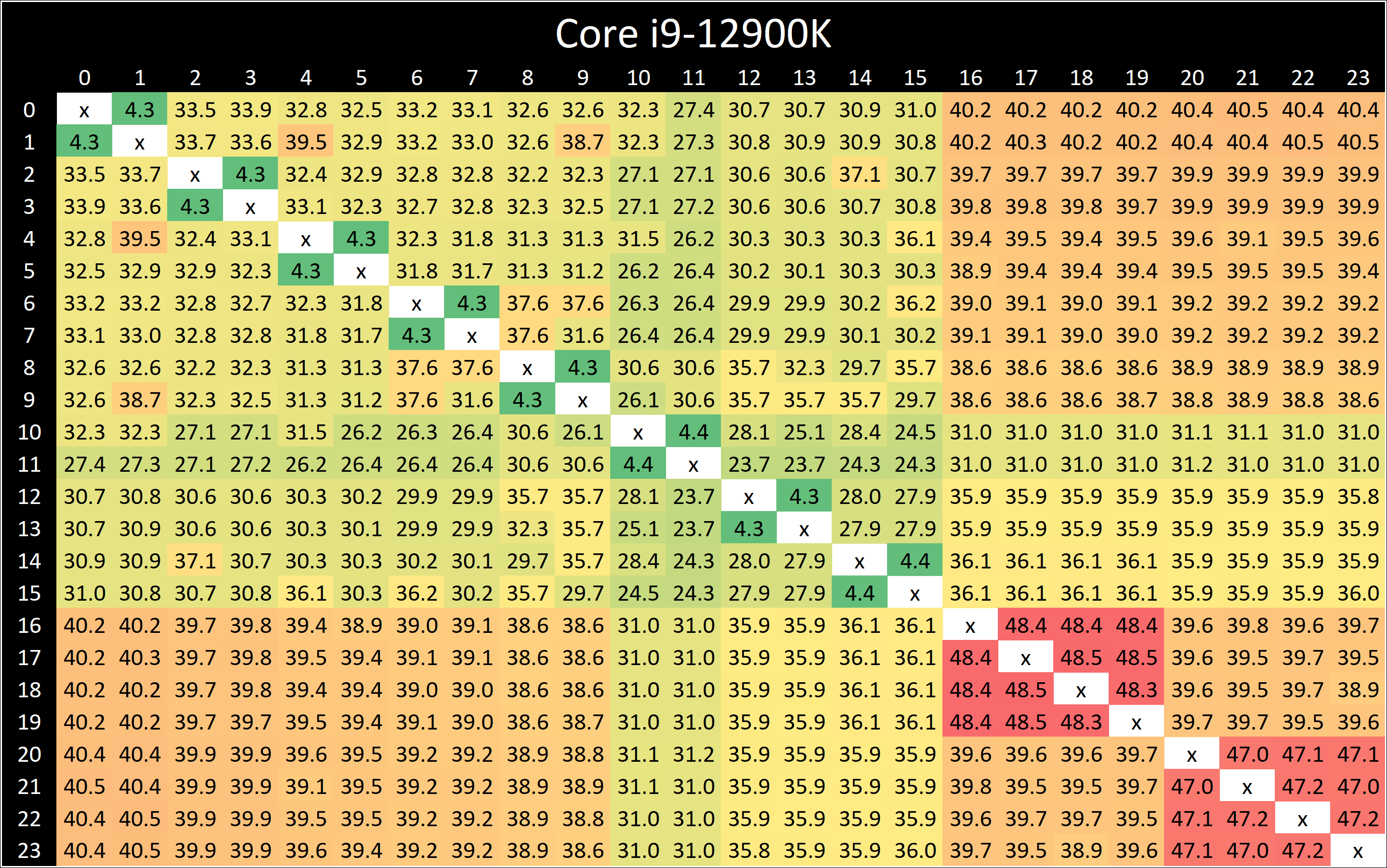
In our core-to-core latency test which showcases the physical topology of the chip, there’s a few things to note. Beginning with the P-cores, which are logically enumerated in the operating system as cores 0 to 15, we can see that latencies are about the same as what we’ve seen on Rocket Lake, although with a few nanosecond differences in the results. The latencies appear to be a bit more topologically uniform, which might indicate that Intel might have finally gotten rid of their uni-directional coherency snoop ring for a bi-directional one.
Latencies between the SMT siblings are also interesting as they decrease from 5.2ns on the Willow Cove cores to 4.3ns on the new Golden Cove cores. The actual L1 access latencies haven’t changed between the two microarchitectures, which means that Intel has improved the LOCK instruction cycle latency.
Between the Golden Cove cores and the smaller Gracemont cores we see higher latencies, as that was to be expected given their lower clock speeds and possible higher L2 overhead of the Gracemont cluster.
What’s however a bit perplexing is that the core-to-core latencies between Gracemont cores is extremely slow, and that’s quite unintuitive as one would have expected coherency between them to be isolated purely on their local L2 cluster. Instead, what seems to be happening is that even between two cores in a cluster, requests have to travel out to the L3 ring, and come back to the very same pathway. That’s quite weird, and we don’t have a good explanation as to why Intel would do this.
Cache Latencies and DDR5 vs DDR4
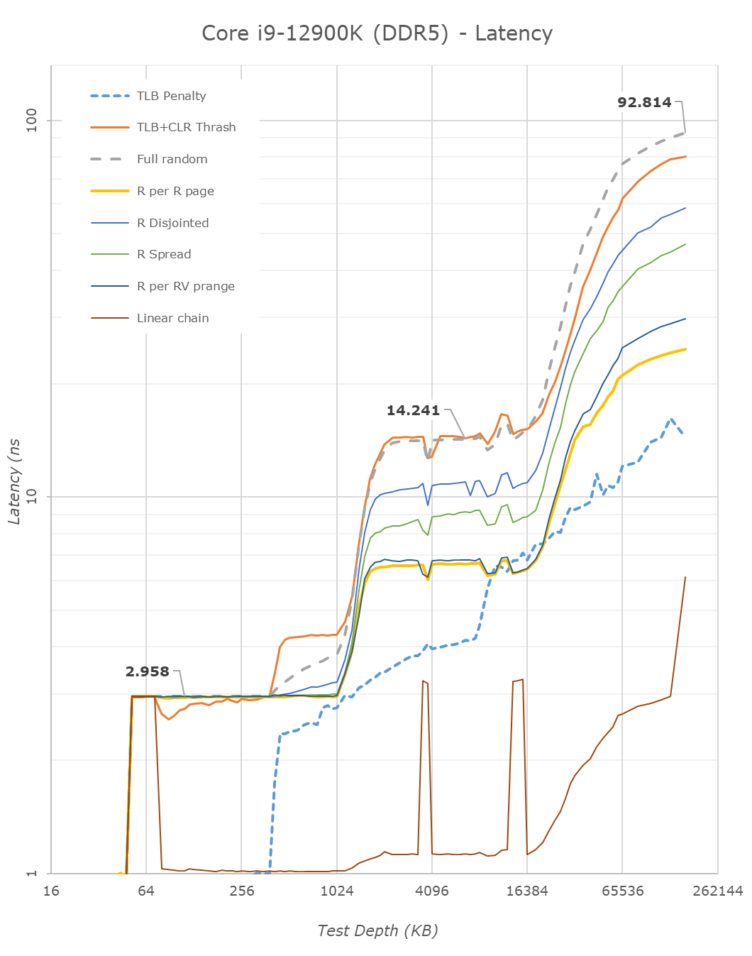
Next up, let’s take a look at the new cache hierarchy of Alder Lake, both from the view of the Golden Cove cores as well as the Gracemont cores, in DDR5 as well as DDR4.
Alder Lake changes up the big cores cache quite considerably. First off, the L1D remains identical – so not much to report there.
On the L2 side of things, compared to Rocket Lake’s Willow Cove cores, Alder Lake’s Golden Cove cores considerably increase the L2 cache from 512KB to 1.25MB. This does come at a 15% latency degradation for this cache, however given the 2.5x increase in size and thus higher hit rates, it’s a good compromise to make.
The Gracemont E-cores have a large 2MB L2 which is shared amongst the 4 cores in a cluster, so things do look quite differently in terms of hierarchy. Here latencies after 192KB do increase for some patterns as it exceeds the 48-page L1 TLB of the cores. Same thing happens at 8MB as the 1024-page L2 TLB is exceeded.
The L3 cache of the chip increases vastly from 16MB in RKL to 30MB in ADL. This increase also does come with a latency increase – at equal test depth, up from 11.59ns to 14.24ns. Intel’s ring and cache slice approach remains considerably slower than AMD’s CCX, which at a similar L3 size of 32MB comes in at 10.34ns for equivalent random-access patterns.
On the DRAM side of things, we can start off with the RKL DDR4 to ADL DDR4 results. The memory latency at 160MB goes up from 85ns to 90ns – generally expected given the larger memory subsystem of the new chip.
Shifting over from DDR4 to the DDR5 results on Alder Lake, at JEDEC speeds, comparing DDR4-3200 CL20 to DDR4-4800 CL40, the officially supported speeds of the chip, we see memory latency only go up to 92.8ns, which is actually below our expectations. In other prefetcher-friendly patterns, latency goes up by a larger 5ns, but still that’s all within reasonable figures, and means that DDR5 latency regressions we feared are overblown, and the chip is able to take advantage of the new memory type without any larger issues.
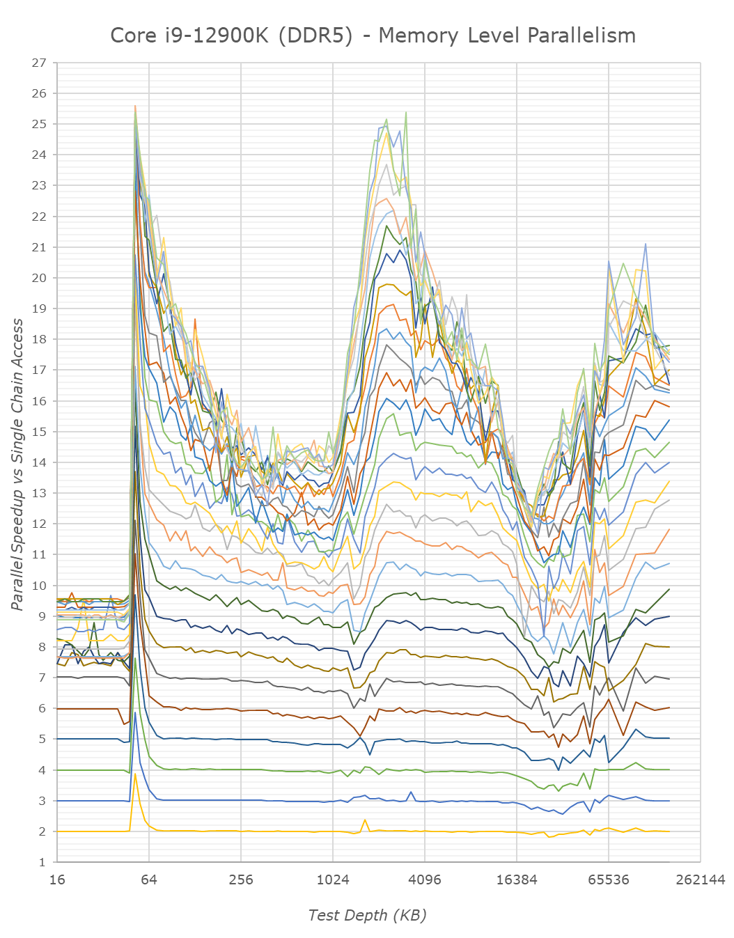
We only ever whip out our memory level parallelism test when there’s a brand-new microarchitecture which changes things quite considerably in regards to how it handles MLP. Alder Lake and its Golden Cove and Gracemont cores are such designs.
Memory level parallelism is the characteristic of a CPU being able to have multiple pending memory accesses – instead of doing things serially, out of order CPUs are able to fetch data from multiple memory locations at the same time. The definition of how many accesses this ends up as, depends on the design within the core, such as MHSR’s, but also the actual parallelism of the various caches as well as the fabric itself. Our test here compares the relative speedup of doing parallel access of random pointer chain chasing – a speedup of 2x means that the core is able to access two chains simultaneously with no degradation of per-element access times. At some point, we’ll be hitting bottlenecks of the various memory elements of the core and memory subsystem. A higher MLP speedup allows for faster execution in workloads which have data-level parallelism, and also improves the ability to hide latency in terms of performance.
Intel’s Golden Cove core is here a massive uplift in terms of its MLP capabilities. The L2 cache of the chip, because it’s so much larger, likely also has a lot more physical banks to it, likely allowing more parallel accesses.
On the L3 cache, Intel also notably mentioned that the new design is able to handle more outstanding transfers, as we immediately see this in the results of Golden Cove. Our test here only tracked up to 30 parallel accesses and we didn’t have time to check out a more extended test, but it does seem the core would be able to hit higher figures – at least until it hits TLB limits, where things slow down. The MLP capabilities here are similar, if not greater, than what AMD showcases in their Zen CPUs, something we had noted as being a strength of their microarchitecture.
MLP at deeper DRAM regions is essentially double that of Rocket Lake – at least on the DDR5 variant of Alder Lake. The DDR4 results reduce the MLP advantage, likely because the chip has to deal with only 2 memory channels rather than 4 on the DDR5 test, this allows the DDR5 variant more parallel sparse accesses to DRAM banks. Interestingly, Intel still doesn’t do as well as AMD even with DDR5 – I’m not sure where exactly the differences stem from, but it must be further down the fabric and memory controller side of things.
From the E-core Gracemont cores, the results also look good, albeit the L3 parallelism looks lower – maybe that’s a limit of the outstanding requests from the L2 cluster of the GRM cores – or maybe some interface limitation.
I think the MLP improvements of Alder Lake here are extremely massive, and represent a major jump in terms of memory performance of the design, something which undoubtedly lead to larger IPC gains for the new microarchitecture.


474 Comments
View All Comments
mode_13h - Sunday, November 7, 2021 - link
I'm not even going to say this is a bad idea. The problem is that it's a big change and Intel normally prepares the software developer community for big new ISA extensions a year+ in advance!Again, what you're talking about is an ABI change, which is a big deal. Not only that, but to require code to handle dynamically switching between AVX2 and AVX-512 paths means that it can't use different datastructures for each codepath. It even breaks the task pre-emption model, since there need to be some limitations on where the code needs to have all its 512-bit registers flushed so it can handle switching to the AVX2 codepath (or vice versa).
This adds a lot of complexity to the software, and places a greater testing burden on software developers. All for (so far) one CPU. It just seems a bit much, and I'm sure a lot of software companies would just decide not to touch AVX-512 until things settle down.
GeoffreyA - Sunday, November 7, 2021 - link
My view on this topic is that Intel made a sound decision disabling AVX512. Some of the comments are framing it as if they made a mistake, because the tech community discovered it was still there, but I don't see any problem. Only, the wording was at fault, this controversial "fused off" statement. And actually, the board makers are at fault, too, enabling a hidden feature and causing more confusion.On the question of whether it's desirable, allowing one core with the instructions and another without, would've been a recipe for disaster---and that, too, for heaven knows what gain. The simplest approach was bringing both cores onto the same footing. Indeed, I think this whole P/E paradigm is worthless, adding complexity for minimal gain.
Oxford Guy - Monday, November 8, 2021 - link
‘Intel made a sound decision disabling AVX512’That’s not what happened.
O-o-o-O - Sunday, November 7, 2021 - link
Really? Our tech guys tried out Xeon Phi but couldn't make use of it. Years later, Xeon Phi was abruptly discontinued due to lack of demand. GPGPUs are much easier to handle.Yeah, coding cost and risks aside, it's interesting to see complex work of art in the modern CPU. But I'd rather wish for expansion of GPU support (like shared memory and higher band-width).
kwohlt - Sunday, November 7, 2021 - link
My understanding is that Raptor Lake's change is replacing Golden Cover P cores with Raptor Cove P cores, doubling Gracemont E-Cores per SKU, and using the same Intel 7 process. Granted, it's all leaks at this point, but with Gracemont being reused for Raptor Lake, I don't expect AVX-512 next year either.mode_13h - Monday, November 8, 2021 - link
> Raptor Lake's change is ... doubling Gracemont E-Cores ... using the same Intel 7 process.I was merely speculating that this *might* just be a transient problem. If they're using the same process node for Raptor Lake, which seems very plausible, then it's understandable if they don't want to increase the size or complexity of their E-cores.
However, there's some precedent, in the form of Knights Landing, where Intel bolted on dual AVX-512 pipelines + SMT4 to a Silvermont Atom core. And with a more mature Intel 7 node, perhaps the yield will support the additional area needed for just a single pipe + 512-bit registers. And let's not forget how Intel increased the width of Goldmont, yet simply referred to it as Goldmont+.
So, maybe Raptor Lake will use Gracemont+ cores that are augmented with AVX-512. We can hope.
GURU7OF9 - Saturday, November 6, 2021 - link
The is by far the best review I have read so far.A great comparison I would love to see just out of curiouslty would be to see P core only benchmarks and then e core only benchmarks! We could gain a much better understanding of the capabilities and performance of both .
This would bring a little bit of familiarity back to benchmarking .
nunya112 - Saturday, November 6, 2021 - link
the only info provided was its on intels new process 7 node. what does that mean? are they using TSMC and at 7nm? or did they finally crack 7nm at Intel?mode_13h - Sunday, November 7, 2021 - link
"Intel 7" is the process node formerly known as "10 nm ESF" (Enhanced SuperFin), which is the 4th generation 10 nm process, counting by the revisions they've introduced between the different products based on it. They like to pretend that Cannon Lake didn't happen, but that's why Ice Lake was actually 10 nm+ (2nd gen).They rebranded 10 nm ESF as "Intel 7" for marketing reasons, as explained here:
https://www.anandtech.com/show/16823/intel-acceler...
Hossein - Sunday, November 7, 2021 - link
It's funny that most reviewers are conveniently silent about the fact that there are quite a 'few' games which are incompatible AL.