The Intel 12th Gen Core i9-12900K Review: Hybrid Performance Brings Hybrid Complexity
by Dr. Ian Cutress & Andrei Frumusanu on November 4, 2021 9:00 AM ESTCPU Tests: Core-to-Core and Cache Latency, DDR4 vs DDR5
Starting off with the first of our synthetic tests, we’re looking into the memory subsystem of Alder Lake-S, as Intel has now included a great deal of changes to the microarchitecture, both on a chip-level, as well as on a platform-level due to the new DDR5 memory compatibility.
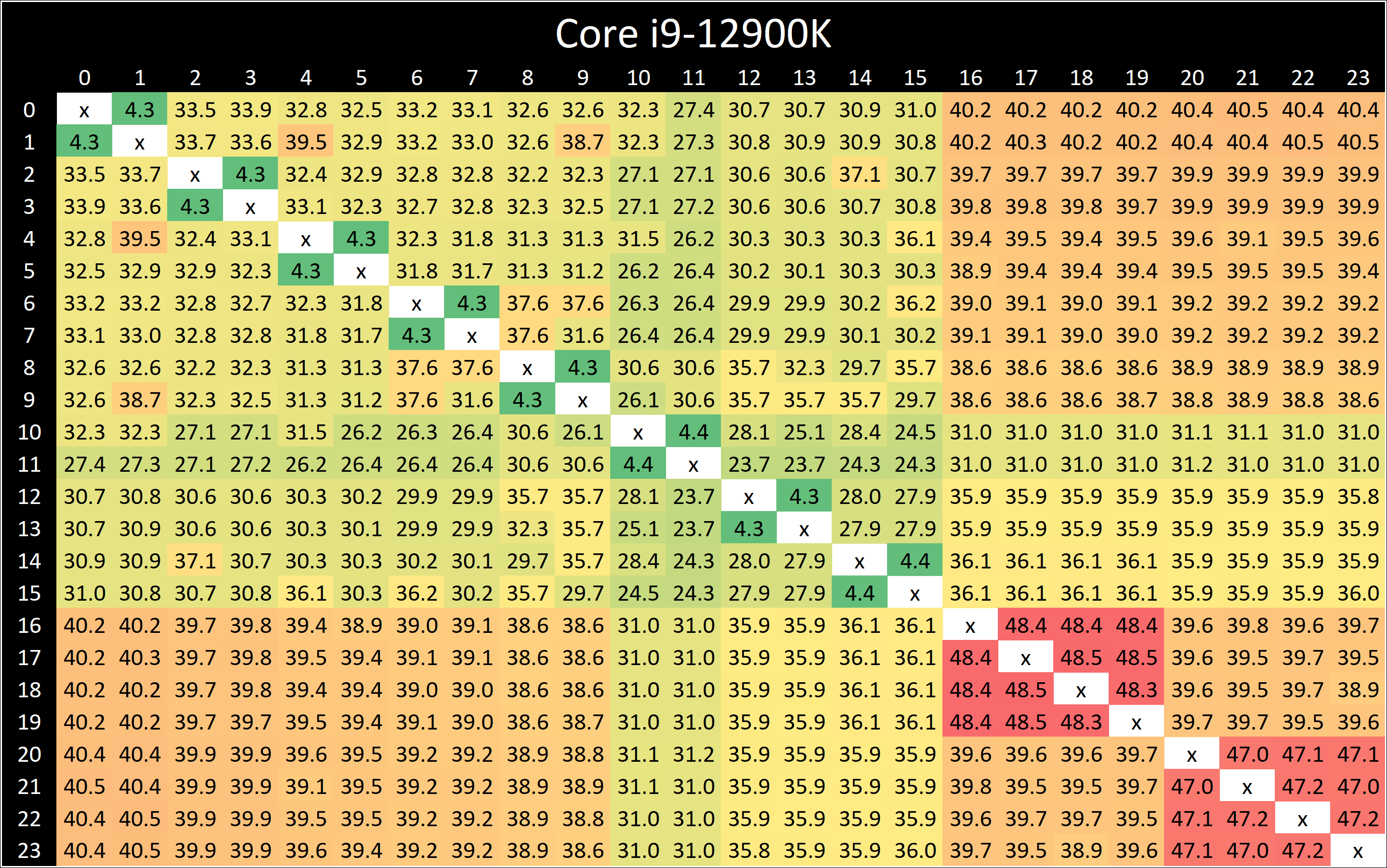
In our core-to-core latency test which showcases the physical topology of the chip, there’s a few things to note. Beginning with the P-cores, which are logically enumerated in the operating system as cores 0 to 15, we can see that latencies are about the same as what we’ve seen on Rocket Lake, although with a few nanosecond differences in the results. The latencies appear to be a bit more topologically uniform, which might indicate that Intel might have finally gotten rid of their uni-directional coherency snoop ring for a bi-directional one.
Latencies between the SMT siblings are also interesting as they decrease from 5.2ns on the Willow Cove cores to 4.3ns on the new Golden Cove cores. The actual L1 access latencies haven’t changed between the two microarchitectures, which means that Intel has improved the LOCK instruction cycle latency.
Between the Golden Cove cores and the smaller Gracemont cores we see higher latencies, as that was to be expected given their lower clock speeds and possible higher L2 overhead of the Gracemont cluster.
What’s however a bit perplexing is that the core-to-core latencies between Gracemont cores is extremely slow, and that’s quite unintuitive as one would have expected coherency between them to be isolated purely on their local L2 cluster. Instead, what seems to be happening is that even between two cores in a cluster, requests have to travel out to the L3 ring, and come back to the very same pathway. That’s quite weird, and we don’t have a good explanation as to why Intel would do this.
Cache Latencies and DDR5 vs DDR4
Next up, let’s take a look at the new cache hierarchy of Alder Lake, both from the view of the Golden Cove cores as well as the Gracemont cores, in DDR5 as well as DDR4.
Alder Lake changes up the big cores cache quite considerably. First off, the L1D remains identical – so not much to report there.
On the L2 side of things, compared to Rocket Lake’s Willow Cove cores, Alder Lake’s Golden Cove cores considerably increase the L2 cache from 512KB to 1.25MB. This does come at a 15% latency degradation for this cache, however given the 2.5x increase in size and thus higher hit rates, it’s a good compromise to make.
The Gracemont E-cores have a large 2MB L2 which is shared amongst the 4 cores in a cluster, so things do look quite differently in terms of hierarchy. Here latencies after 192KB do increase for some patterns as it exceeds the 48-page L1 TLB of the cores. Same thing happens at 8MB as the 1024-page L2 TLB is exceeded.
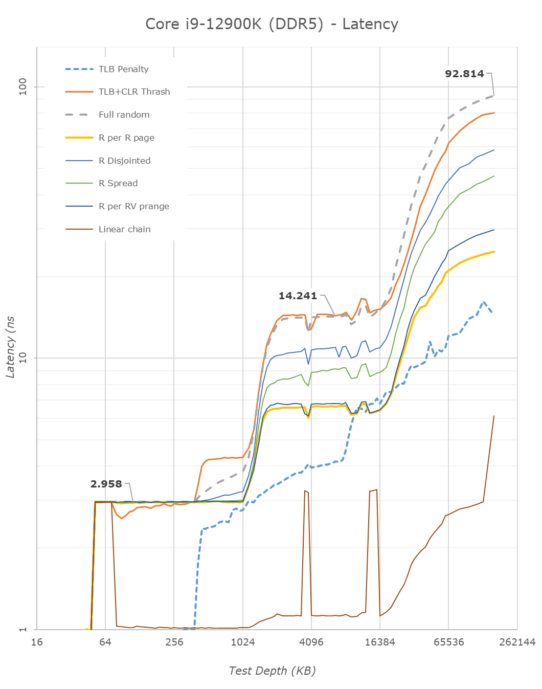
The L3 cache of the chip increases vastly from 16MB in RKL to 30MB in ADL. This increase also does come with a latency increase – at equal test depth, up from 11.59ns to 14.24ns. Intel’s ring and cache slice approach remains considerably slower than AMD’s CCX, which at a similar L3 size of 32MB comes in at 10.34ns for equivalent random-access patterns.
On the DRAM side of things, we can start off with the RKL DDR4 to ADL DDR4 results. The memory latency at 160MB goes up from 85ns to 90ns – generally expected given the larger memory subsystem of the new chip.
Shifting over from DDR4 to the DDR5 results on Alder Lake, at JEDEC speeds, comparing DDR4-3200 CL20 to DDR4-4800 CL40, the officially supported speeds of the chip, we see memory latency only go up to 92.8ns, which is actually below our expectations. In other prefetcher-friendly patterns, latency goes up by a larger 5ns, but still that’s all within reasonable figures, and means that DDR5 latency regressions we feared are overblown, and the chip is able to take advantage of the new memory type without any larger issues.
We only ever whip out our memory level parallelism test when there’s a brand-new microarchitecture which changes things quite considerably in regards to how it handles MLP. Alder Lake and its Golden Cove and Gracemont cores are such designs.
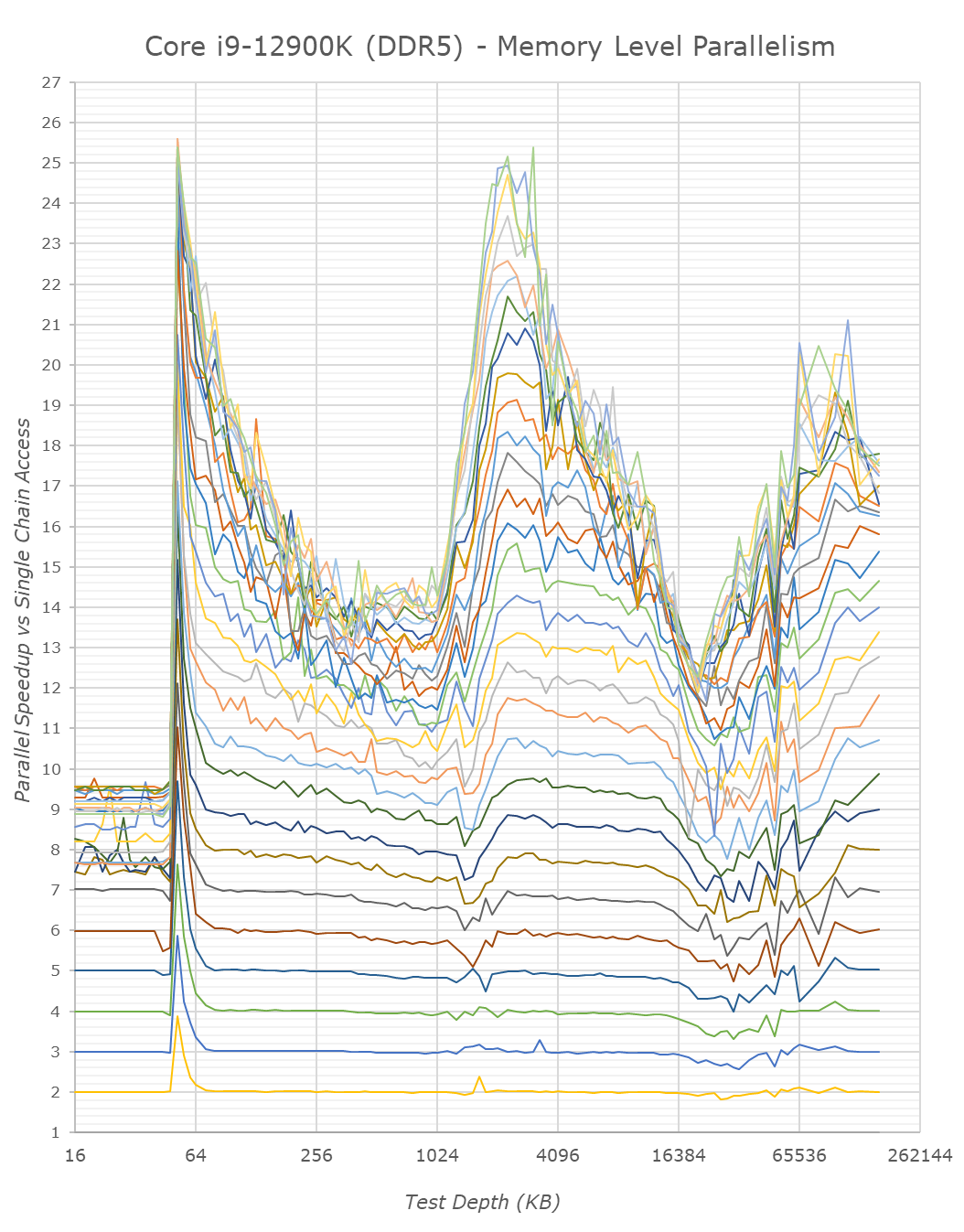
Memory level parallelism is the characteristic of a CPU being able to have multiple pending memory accesses – instead of doing things serially, out of order CPUs are able to fetch data from multiple memory locations at the same time. The definition of how many accesses this ends up as, depends on the design within the core, such as MHSR’s, but also the actual parallelism of the various caches as well as the fabric itself. Our test here compares the relative speedup of doing parallel access of random pointer chain chasing – a speedup of 2x means that the core is able to access two chains simultaneously with no degradation of per-element access times. At some point, we’ll be hitting bottlenecks of the various memory elements of the core and memory subsystem. A higher MLP speedup allows for faster execution in workloads which have data-level parallelism, and also improves the ability to hide latency in terms of performance.
Intel’s Golden Cove core is here a massive uplift in terms of its MLP capabilities. The L2 cache of the chip, because it’s so much larger, likely also has a lot more physical banks to it, likely allowing more parallel accesses.
On the L3 cache, Intel also notably mentioned that the new design is able to handle more outstanding transfers, as we immediately see this in the results of Golden Cove. Our test here only tracked up to 30 parallel accesses and we didn’t have time to check out a more extended test, but it does seem the core would be able to hit higher figures – at least until it hits TLB limits, where things slow down. The MLP capabilities here are similar, if not greater, than what AMD showcases in their Zen CPUs, something we had noted as being a strength of their microarchitecture.
MLP at deeper DRAM regions is essentially double that of Rocket Lake – at least on the DDR5 variant of Alder Lake. The DDR4 results reduce the MLP advantage, likely because the chip has to deal with only 2 memory channels rather than 4 on the DDR5 test, this allows the DDR5 variant more parallel sparse accesses to DRAM banks. Interestingly, Intel still doesn’t do as well as AMD even with DDR5 – I’m not sure where exactly the differences stem from, but it must be further down the fabric and memory controller side of things.
From the E-core Gracemont cores, the results also look good, albeit the L3 parallelism looks lower – maybe that’s a limit of the outstanding requests from the L2 cluster of the GRM cores – or maybe some interface limitation.
I think the MLP improvements of Alder Lake here are extremely massive, and represent a major jump in terms of memory performance of the design, something which undoubtedly lead to larger IPC gains for the new microarchitecture.


474 Comments
View All Comments
Oxford Guy - Sunday, November 7, 2021 - link
‘or maybe switch off their E-cores and enable AVX-512 in BIOS’This from exactly the same person who posted, just a few hours ago, that it’s correct to note that that option can disappear and/or be rendered non-functional.
I am reminded of your contradictory posts about ECC where you mocked advocacy for it (‘advocacy’ being merely its mention) and proceeded to claim you ‘wish’ for more ECC support.
Once again, it’s helpful to have a grasp of what one actually believes prior to posting. Allocating less effort to posting puerile insults and more toward substance is advised.
mode_13h - Sunday, November 7, 2021 - link
> This from exactly the same person who posted, just a few hours ago, that it’s> correct to note that that option can disappear and/or be rendered non-functional.
You need to learn to distinguish between what Intel has actually stated vs. the facts as we wish them to be. In the previous post you reference, I affirmed your acknowledgement that the capability disappearing would be consistent with what Intel has actually said, to date.
In the post above, I was leaving open the possibility that *maybe* Intel is actually "cool" with there being a BIOS option to trade AVX-512 for E-cores. We simply don't know how Intel feels about that, because (to my knowledge) they haven't said.
When I clarify the facts as they stand, don't confuse that with my position on the facts as I wish them to be. I can simultaneously acknowledge one reality, which maintaining my own personal preference for a different reality.
This is exactly what happened with the ECC situation: I was clarifying Intel's practice, because your post indicated uncertainty about that fact. It was not meant to convey my personal preference, which I later added with a follow-on post.
Having to clarify this to an "Oxford Guy" seems a bit surprising, unless you meant like Oxford Mississippi.
> you mocked advocacy
It wasn't mocking. It was clarification. And your post seemed more to express befuddlement than expressive of advocacy. It's now clear that your post was a poorly-executed attempt at sarcasm.
Once again, it's helpful not to have your ego so wrapped up in your posts that you overreact when someone tries to offer a factual clarification.
Oxford Guy - Monday, November 8, 2021 - link
I now skip to the bottom of your posts If I see more of the same preening and posing, I spare myself the rest of the nonsense.mode_13h - Tuesday, November 9, 2021 - link
> If I see more of the same preening and posing, I spare myself the rest of the nonsense.Then I suggest you don't read your own posts.
I can see that you're highly resistant to reason and logic. Whenever I make a reasoned reply, you always hit back with some kind of vague meta-critique. If that's all you've got, it can be seen as nothing less than a concession.
O-o-o-O - Saturday, November 6, 2021 - link
Anyone talking about dumping x64 ISA?I don't see AVX-512 a good solution. Current x64 chips are putting so much complexity in CPU with irrational clock speed that migrating process-node further into Intel4 on would be a nightmare once again.
I believe most of the companies with in-house developers expect the end of Xeon-era is quite near, as most of the heavy computational tasks are fully optimized for GPUs and that you don't want coal burning CPUs.
Even if it doesn't come in 5 year time-frame, there's a real threat and have to be ahead of time. After all, x86 already extended its life 10+ years when it could have been discontinued. Now it's really a dinosaur. If so, non-server applications would follow the route as well.
We want more simple / solid / robust base with scalability. Not an unreliable boost button that sometimes do the trick.
SystemsBuilder - Saturday, November 6, 2021 - link
I don't see AVX-512 that negatively it is just the same as AVX2 but double the vectors size and a with a richer instruction set. I find it pretty cool to work with especially when you've written some libraries that can take advantage of it. As I wrote before, it looks like Golden cove got AVX-512 right based on what Ian and Andrei uncovered. 0 negative offset (e.g. running at full speed), power consumption not much more than AVX2, and it supports both FP16 and BP16 vectors! I think that's pretty darn good! I can work with that! Now I want my Sapphire rapids with 32 or 48 Golden cove P cores! No not fall 2022 i want it now! lolmode_13h - Saturday, November 6, 2021 - link
> When you optimize code today (for pre Alder lake CPUs) to take advantage> of AVX-512 you need to write two paths (at least).
Ah, so your solution depends on application software changes, specifically requiring them to do more work. That's not viable for the timeframe of concern. And especially not if its successor is just going to add AVX-512 to the E-cores, within a year or so.
> There are many levels of AVX-512 support and effectively you need write customized
> code for each specific CPUID
But you don't expect the capabilities to change as a function of which thread is running, or within a program's lifetime! What you're proposing is very different. You're proposing to change the ABI. That's a big deal!
> It is absolutely possible and it will come with time.
Or not. ARM's SVE is a much better solution.
> I think in the future P and E cores might have more than just AVX-512 that is different
On Linux, using AMX will require a thread to "enable" it. This is a little like what you're talking about. AMX is a big feature, though, and unlike anything else. I don't expect to start having to enable every new ISA extension I want to use, or query how many hyperthreads actually support - this becomes a mess when you start dealing with different libraries that have these requirements and limitations.
Intel's solution isn't great, but it's understandable and it works. And, in spite of it, they still delivered a really nice-performing CPU. I think it's great if technically astute users have/retain the option to trade E-cores for AVX-512 (via BIOS), but I think it's kicking a hornets nest to go down the path of having a CPU with asymmetrical capabilities among its cores.
Hopefully, Raptor Lake just adds AVX-512 to the E-cores and we can just let this issue fade into the mists of time, like other missteps Intel & others have made.
SystemsBuilder - Saturday, November 6, 2021 - link
I too believe AVX-512 exclusion in the E cores it is transitory. next gen E cores may include it and the issue goes away for AVX-512 at least (Raptor Lake?). Still there will be other features that P have but E won't have so the scheduler needs to be adjusted for that. This will continue to evolve with every generation of E and P cores - because they are here to stay.I read somewhere a few months ago but right now i do not remember where (maybe on Anandtech not sure) that the AVX-512 transistor budget is quite small (someone measured it on the die) so not really a big issue in terms of area.
AMX is interesting because where AVX-512 are 512 bit vectors, AMX is making that 512x512 bit matrices or tiles as intel calls it. Reading the spec on AMX you have BF16 tiles which is awesome if you're into neural nets. Of course gpus will still perform better with matrix calculations (multiplications) but the benefit with AMX is that you can keep both the general CPU code and the matrix specific code inside the CPU and can mix the code seamlessly and that's gonna be very cool - you cut out the latency between GPU and CPU (and no special GPU API's are needed). but of course you can still use the GPU when needed (sometimes it maybe faster to just do a matrix- matrix add for instance just inside the CPU with the AMX tiles) - more flexibility.
Anyway, I do think we will run into a similar issue with AMX as we have the AVX-512 on Alder Lake and therefore again the scheduler needs to become aware of each cores capabilities and each piece of code need to state what type of core they prefer to run on: AVX2, AVX-512, AMX capable core etc (the compliers job). This way the scheduler can do the best job possible with every thread.
There will be some teething for a while but i think this is the direction it is going.
mode_13h - Sunday, November 7, 2021 - link
The difference is that AMX is new. It's also much more specialized, as you point out. But that means that they can place new hoops for code to jump through, in order to use it.It's very hard to put a cat like AVX-512 back in the bag.
SystemsBuilder - Saturday, November 6, 2021 - link
To be clear, I also want to add that the way code is written today (in my organization) pre Alder Lake code base. Every time we write a code path for AVX512 we need to write a fallback code path incase the CPU is not AVX-512 capable. This is standard (unless you can control the execution H/W 100% - i.e. the servers).Does not mean all code has to be duplicated but the inner loops where the 80%/20% rule (i.e. 20% of the code that consumes 80% of the time, which in my experience often becomes like the 99%/1% rule) comes into play that's where you write two code paths:
1 for AVX-512 in case it CPU is capable and
2 with just AVX2 in case CPU is not capable
mostly this ends up being just as I said the inner most loops, and there are excellent broadly available templates to use for this.
Just from a pure comp sci perspective it is quite interesting to vectorize code and see the benefits - pretty cool actually.