Apple's M1 Pro, M1 Max SoCs Investigated: New Performance and Efficiency Heights
by Andrei Frumusanu on October 25, 2021 9:00 AM EST- Posted in
- Laptops
- Apple
- MacBook
- Apple M1 Pro
- Apple M1 Max
Huge Memory Bandwidth, but not for every Block
One highly intriguing aspect of the M1 Max, maybe less so for the M1 Pro, is the massive memory bandwidth that is available for the SoC.
Apple was keen to market their 400GB/s figure during the launch, but this number is so wild and out there that there’s just a lot of questions left open as to how the chip is able to take advantage of this kind of bandwidth, so it’s one of the first things to investigate.
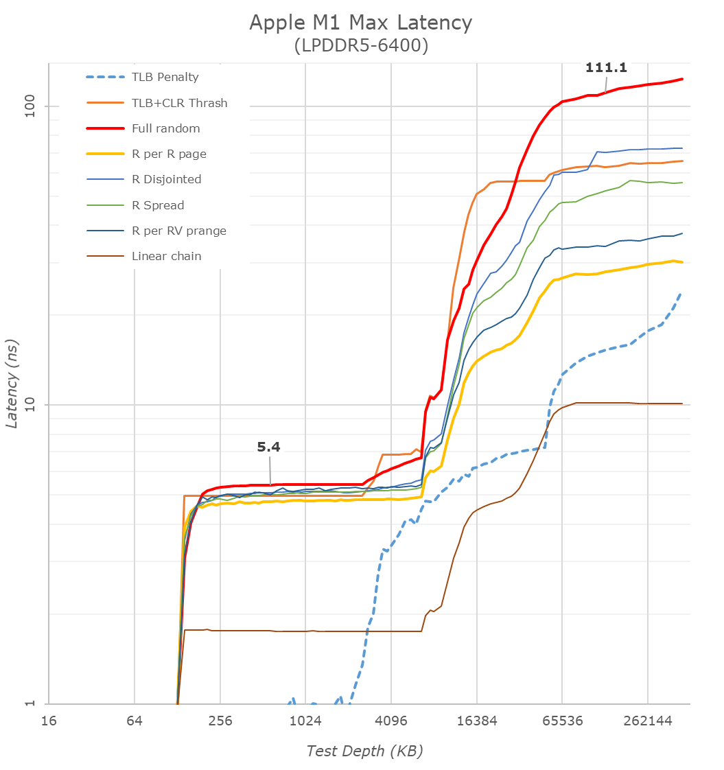
Starting off with our memory latency tests, the new M1 Max changes system memory behaviour quite significantly compared to what we’ve seen on the M1. On the core and L2 side of things, there haven’t been any changes and we consequently don’t see much alterations in terms of the results – it’s still a 3.2GHz peak core with 128KB of L1D at 3 cycles load-load latencies, and a 12MB L2 cache.
Where things are quite different is when we enter the system cache, instead of 8MB, on the M1 Max it’s now 48MB large, and also a lot more noticeable in the latency graph. While being much larger, it’s also evidently slower than the M1 SLC – the exact figures here depend on access pattern, but even the linear chain access shows that data has to travel a longer distance than the M1 and corresponding A-chips.
DRAM latency, even though on paper is faster for the M1 Max in terms of frequency on bandwidth, goes up this generation. At a 128MB comparable test depth, the new chip is roughly 15ns slower. The larger SLCs, more complex chip fabric, as well as possible worse timings on the part of the new LPDDR5 memory all could add to the regression we’re seeing here. In practical terms, because the SLC is so much bigger this generation, workloads latencies should still be lower for the M1 Max due to the higher cache hit rates, so performance shouldn’t regress.
A lot of people in the HPC audience were extremely intrigued to see a chip with such massive bandwidth – not because they care about GPU or other offload engines of the SoC, but because the possibility of the CPUs being able to have access to such immense bandwidth, something that otherwise is only possible to achieve on larger server-class CPUs that cost a multitude of what the new MacBook Pros are sold at. It was also one of the first things I tested out – to see exactly just how much bandwidth the CPU cores have access to.
Unfortunately, the news here isn’t the best case-scenario that we hoped for, as the M1 Max isn’t able to fully saturate the SoC bandwidth from just the CPU side;
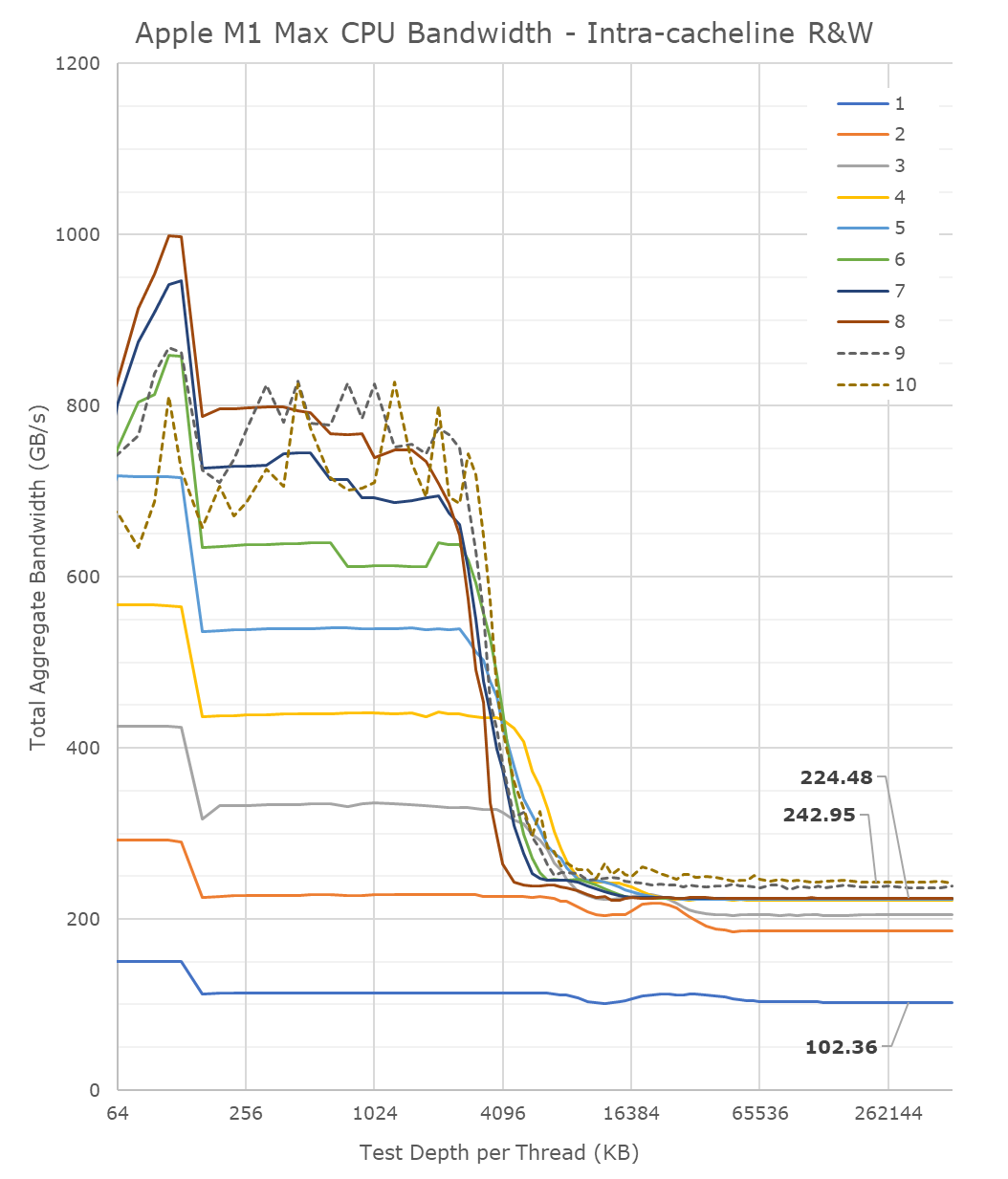
From a single core perspective, meaning from a single software thread, things are quite impressive for the chip, as it’s able to stress the memory fabric to up to 102GB/s. This is extremely impressive and outperforms any other design in the industry by multiple factors, we had already noted that the M1 chip was able to fully saturate its memory bandwidth with a single core and that the bottleneck had been on the DRAM itself. On the M1 Max, it seems that we’re hitting the limit of what a core can do – or more precisely, a limit to what the CPU cluster can do.
The little hump between 12MB and 64MB should be the SLC of 48MB in size, the reduction in BW at the 12MB figure signals that the core is somehow limited in bandwidth when evicting cache lines back to the upper memory system. Our test here consists of reading, modifying, and writing back cache lines, with a 1:1 R/W ratio.
Going from 1 core/threads to 2, what the system is actually doing is spreading the workload across the two performance clusters of the SoC, so both threads are on their own cluster and have full access to the 12MB of L2. The “hump” after 12MB reduces in size, ending earlier now at +24MB, which makes sense as the 48MB SLC is now shared amongst two cores. Bandwidth here increases to 186GB/s.
Adding a third thread there’s a bit of an imbalance across the clusters, DRAM bandwidth goes to 204GB/s, but a fourth thread lands us at 224GB/s and this appears to be the limit on the SoC fabric that the CPUs are able to achieve, as adding additional cores and threads beyond this point does not increase the bandwidth to DRAM at all. It’s only when the E-cores, which are in their own cluster, are added in, when the bandwidth is able to jump up again, to a maximum of 243GB/s.
While 243GB/s is massive, and overshadows any other design in the industry, it’s still quite far from the 409GB/s the chip is capable of. More importantly for the M1 Max, it’s only slightly higher than the 204GB/s limit of the M1 Pro, so from a CPU-only workload perspective, it doesn’t appear to make sense to get the Max if one is focused just on CPU bandwidth.
That begs the question, why does the M1 Max have such massive bandwidth? The GPU naturally comes to mind, however in my testing, I’ve had extreme trouble to find workloads that would stress the GPU sufficiently to take advantage of the available bandwidth. Granted, this is also an issue of lacking workloads, but for actual 3D rendering and benchmarks, I haven’t seen the GPU use more than 90GB/s (measured via system performance counters). While I’m sure there’s some productivity workload out there where the GPU is able to stretch its legs, we haven’t been able to identify them yet.
That leaves everything else which is on the SoC, media engine, NPU, and just workloads that would simply stress all parts of the chip at the same time. The new media engine on the M1 Pro and Max are now able to decode and encode ProRes RAW formats, the above clip is a 5K 12bit sample with a bitrate of 1.59Gbps, and the M1 Max is not only able to play it back in real-time, it’s able to do it at multiple times the speed, with seamless immediate seeking. Doing the same thing on my 5900X machine results in single-digit frames. The SoC DRAM bandwidth while seeking around was at around 40-50GB/s – I imagine that workloads that stress CPU, GPU, media engines all at the same time would be able to take advantage of the full system memory bandwidth, and allow the M1 Max to stretch its legs and differentiate itself more from the M1 Pro and other systems.


493 Comments
View All Comments
celeste_P - Tuesday, October 26, 2021 - link
Does any one know where can I find the policy about translating/reprinting the article? Do AnandTech allow such behavior? What are the policies that one needs to follow?This article is quite interesting and I want to translate/publish it on Chinese website to share with a broader range of people
colinstalter - Wednesday, October 27, 2021 - link
Why not just share the URL on the Chinese page? Do people in China not have translator functions built into their web browsers like Chrome does?celeste_P - Wednesday, October 27, 2021 - link
Of course they do XDBut as you can imagine, the quality of machine translation won't be that great, especially considering all these domain specific terms within this article.
ABR - Tuesday, October 26, 2021 - link
An excellent review.ajmas - Tuesday, October 26, 2021 - link
Given the number of games already available and running on iOS, I wonder how much work would be involved in making them available on macOS?As for effective performance, I am eagerly waiting to see what the real world tests reveal, since specs only say so much.
mandirabl - Wednesday, October 27, 2021 - link
As a developer, technically you don't have to do much, just re-compile the game and check another box (for Mac), basically.The problem is: iOS games are mostly touch-focused, whereas macOS is mouse-first. So they have to check if that translates without changing anything. If it does, it's a matter of a couple of minutes. If it doesn't translate well ... they have a choice to release it anyway or blocking access on macOS. Yes, developers have to actually decide against releasing their app/game for macOS - if they don't do anything in that regard, the app/game simply shows up in an App Store search on a Mac.
Kevin45 - Tuesday, October 26, 2021 - link
Apple's goal is very simple: If you are going to provide SW tools for Pro users of the MacOS platform, you write to Metal - period.It IS the most superior way to take advantage of what Apple has laid out to developers and Apple's Pro users absolutely want the HW tools they buy to be max'd out by the developers.
Apple has taken an approach Intel and AMD cannot. Unified memory design aside, Apple has looked at it's creative markets and developed sub-cores, which for this Creative focus segment, Apple markets as it's "Media Engine" which has hardware h.264 and hardware ProRes compute, which just crush these formats and codecs.
The argument "Yah, but the CPU and GPU cores aren't the most powerful that one can buy." is still. They don't need to be because they have dedicated cores to where the power needs to be. Sure, in a Wintel world, or Linux space, more powerful GPU and CPU cores is all they've got. So when talking those worlds indeed that's the correct argument. Not when talking Apple HW with Apple silicon.
Intel has fought nVIDIA to have their beefier and beefier cores do heavy lifting, while nVIDA wants the GPU to be the most important play in the mix. Apple has broken out their SoC into many sub-sets to meet the high compute needs of it's user base.
Now more than ever, developers that have drug their feet, need to get onboard. As companies continue to show off - such as Apple with FCP, Motion and Compressor optimized apps for the hardware, even DaVinci (niche player but powerful), they put pressure on other players such as sloth-boy Adobe, to get going and truly write for Apple's tools that take advantage of such well thought out HW + SW combo.
richardnpaul - Tuesday, October 26, 2021 - link
The article comes across a bit fanbioy. (yes, yes I know that this is usually the case here but I just wanted to say it out loud again). See below for why.You have covered in depth things like how the increased L3 design between Zen2 and 3 can cause big jumps in performance and what was missing here was discussion of how the 24/48MB cache between the memory interface impacts performance especially when using the GPU (we've seen this last year AMD's designs doing exactly this to improve performance of their designs by reducing the impact of calling out to the slow GDDR6 RAM.)
The GPU is nothing special. 10Tflops at 1.3GHz puts it around the same class as a Vega64, a 14nm design, which similarly used RAM packaged on an interposer with the GPU (being 14nm it was big, 5nm makes it much more reasonable). With the buffer cache I'd expect it might perform better, also the CPUs will bump up performance (just look at how much more FPS you get with Zen3 over Zen2 and with Zen3 with vcache it'll be another 15% more on top from exactly the same GPU hardware and that's with the CPU and GPU having to talk over PCI-E).
Also, Apple have made themselves second class gaming citizens with their decision to build Mantle and enforce it as the only API (I may be mistaken here but as far as I'm aware the whole reason for Molten is because you have to use Metal on MacOS and developers have introduced this Vulkan to Metal shim to ease porting). Also, as I understand it, you can't connect external dGPUs via Thunderbolt to provide comparisons. Apple's vendor lock-in at it's worst (have I mentioned that Apple are their own worst enemy a lot of the time?)
As such the gaming performance doesn't surprise me, this is a technically much slower and inferior GPU to AMD and nVIDIAs current designs on an older process (7nm and 8nm respectively). The cost is that whilst these are faster, they're larger and more power hungry though a die shrink of bring something like an AMD 6600 based chip into the same ballpark.
Also on the 512bit memory interface I'd probably look at it more like 384bit plus 128bit, which is the GPU plus the usual CPU interfaces. The CPU is always gojng to contend for some of that 512bit interface, so you're never going to see 512bit for the GPU, on the other hand, you get what ever the cpu doesn't use for free, which is a great bonus of this design, and if the CPU needs more than a 128bit interface can manage it has access to that too if the GPU isn't heavily loaded on the memory interface.
I kind of expect you guys to cover all this though in the article, not have me railing at the lack of it in the comments section.
richardnpaul - Tuesday, October 26, 2021 - link
Oh and you failed to ever mention that the trade-off of the design is that you need to buy all the RAM you'll ever need up front because it's soldered to the SoC package. The reason that we don't normally see such designs is that the trade-off is potentially expensive unsaleable parts. The cost of these laptops are way above the usual and whilst they have some really nice tech this is one of the other downsides of this design (and the 5nm node and the amount of silicon).OreoCookie - Tuesday, October 26, 2021 - link
Or perhaps Anandtech gave it a glowing review simply because the M1 Max is fast and energy efficient at the same time? In memory intensive benchmarks it was 2-5 x faster than the x86 competition while being more energy efficient. What more do you want?And the article *was* including a Zen 3 mobile part in its comparison and the M1 Max was faster while consuming less energy. Since the V-Cache version of Zen 3 hasn't been released yet, there are no benchmarks for Anandtech to release as they either haven't been run yet or are under embargo.
Lastly, this article is about some of the low-level capabilities of the hardware, not vendor lock-in or whether Metal is better or worse than Vulkan. They did not even test the ML accelerator or hardware codec bits (which is completely fair).