Intel 12th Gen Core Alder Lake for Desktops: Top SKUs Only, Coming November 4th
by Dr. Ian Cutress on October 27, 2021 12:00 PM EST- Posted in
- CPUs
- Intel
- DDR4
- DDR5
- PCIe 5.0
- Alder Lake
- Intel 7
- 12th Gen Core
- Z690
A Hybrid/Heterogeneous Design
Developing a processor with two different types of core is not a new concept – there are billions of smartphones that have exactly that inside them, running Android or iOS, as well as IoT and embedded systems. We’ve also seen it on Windows, cropping up on Qualcomm’s Windows on Snapdragon mobile notebooks, as well as Intel’s previous Lakefield design. Lakefield was the first x86 hybrid design in that context, and Alder Lake is the more mass-market realization of that plan.
A processor with two different types of core disrupts the typical view of how we might assume a computer works. At the basic level, it has been taught that a modern machine is consistent – every CPU has the same performance, processes the same data at the same rate, has the same latency to memory, the same latency to each other, and everything is equal. This is a straightforward homogenous design that’s very easy to write software for.
Once we start considering that not every core has the same latency to memory, moving up to a situation where there are different aspects of a chip that do different things at different speeds and efficiencies, now we move into a heterogeneous design scenario. In this instance, it becomes more complex to understand what resources are available, and how to use them in the best light. Obviously, it makes sense to make it all transparent to the user.

With Intel’s Alder Lake, we have two types of cores: high performance/P-cores, built on the Golden Cove microarchitecture, and high efficiency/E-cores, built on the Gracemont microarchitecture. Each of these cores are designed for different optimization points – P-cores have a super-wide performance window and go for peak performance, while E-cores focus on saving power at half the frequency, or lower, where the P-core might be inefficient.
This means that if there is a background task waiting on data, or something that isn’t latency-sensitive, it can work on the E-cores in the background and save power. When a user needs speed and power, the system can load up the P-cores with work so it can finish the fastest. Alternatively, if a workload is more throughput sensitive than latency-sensitive, it can be split across both P-cores and E-cores for peak throughput.

For performance, Intel lists a single P-core as ~19% better than a core in Rocket Lake 11th Gen, while a single E-core can offer better performance than a Comet Lake 10th Gen core. Efficiency is similarly aimed to be competitive, with Intel saying a Core i9-12900K with all 16C/24T running at a fixed 65 W will equal its previous generation Core i9-11900K 8C/16T flagship at 250 W. A lot of that will be that having more cores at a lower frequency is more efficient than a few cores at peak frequency (as we see in GPUs), however an effective 4x performance per watt improvement requires deeper investigation in our review.
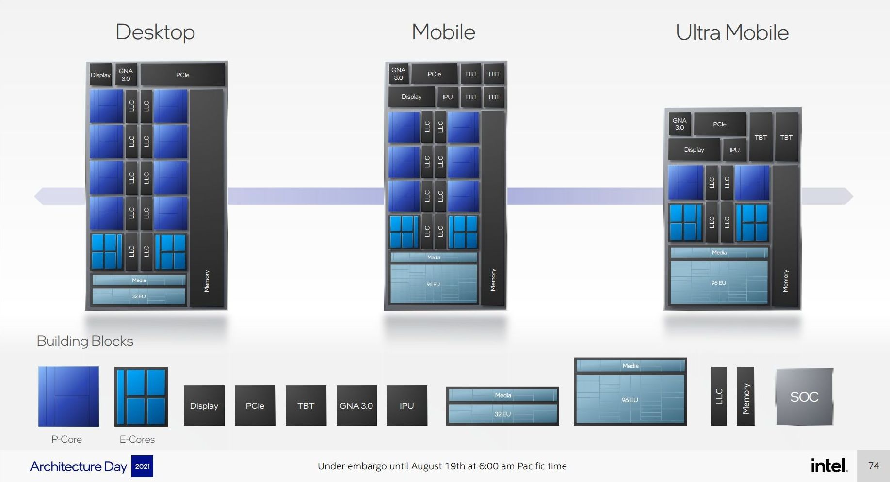
As a result, the P-cores and E-cores look very different. A deeper explanation can be found in our Alder Lake microarchitecture deep dive, but the E-cores end up being much smaller, such that four of them are roughly in the same area as a single P-core. This creates an interesting dynamic, as Intel highlighted back at its Architecture Day: A single P-core provides the best latency-sensitive performance, but a group of E-cores would beat a P-core in performance per watt, arguably at the same performance level.
However, one big question in all of this is how these workloads end up on the right cores in the first place? Enter Thread Director (more on the next page).
A Word on L1, L2, and L3 Cache
Users with an astute eye will notice that Intel’s diagrams relating to core counts and cache amounts are representations, and some of the numbers on a deeper inspection need some explanation.
For the cores, the processor design is physically split into 10 segments.
A segment contains either a P-core or a set of four E-cores, due to their relative size and functionality. Each P-core has 1.25 MiB of private L2 cache, which a group of four E-cores has 2 MiB of shared L2 cache.
This is backed by a large shared L3 cache, totaling 30 MiB. Intel’s diagram shows that there are 10 LLC segments which should mean 3.0 MiB each, right? However, moving from Core i9 to Core i7, we only lose one segment (one group of four E-cores), so how come 5.0 MiB is lost from the total L3? Looking at the processor tables makes less sense.
Please note that the following is conjecture; we're awaiting confirmation from Intel that this is indeed the case.
It’s because there are more than 10 LLC slices – there’s actually 12 of them, and they’re each 2.5 MiB. It’s likely that either each group of E-cores has two slices each, or there are extra ring stops for more cache.
Each of the P-cores has a 2.5 MiB slice of L3 cache, with eight cores making 20 MiB of the total. This leaves 10 MiB between two groups of four E-cores, suggesting that either each group has 5.0 MiB of L3 cache split into two 2.5 MiB slices, or there are two extra LLC slices on Intel’s interconnect.
| Alder Lake Cache | |||||||
| AnandTech | Cores P+E/T |
L2 Cache |
L3 Cache |
IGP | Base W |
Turbo W |
Price $1ku |
| i9-12900K | 8+8/24 | 8x1.25 2x2.00 |
30 | 770 | 125 | 241 | $589 |
| i9-12900KF | 8+8/24 | 8x1.25 2x2.00 |
30 | - | 125 | 241 | $564 |
| i7-12700K | 8+4/20 | 8x1.25 1x2.00 |
25 | 770 | 125 | 190 | $409 |
| i7-12700KF | 8+4/20 | 8x1.25 1x2.00 |
25 | - | 125 | 190 | $384 |
| i5-12600K | 6+4/20 | 6x1.25 1x2.00 |
20 | 770 | 125 | 150 | $289 |
| i5-12600KF | 6+4/20 | 6.125 1x200 |
20 | - | 125 | 150 | $264 |
This is important because moving from Core i9 to Core i7, we lose 4xE-cores, but also lose 5.0 MiB of L3 cache, making 25 MiB as listed in the table. Then from Core i7 to Core i5, two P-cores are lost, totaling another 5.0 MiB of L3 cache, going down to 20 MiB. So while Intel’s diagram shows 10 distinct core/LLC segments, there are actually 12. I suspect that if both sets of E-cores are disabled, so we end up with a processor with eight P-cores, 20 MiB of L3 cache will be shown.


395 Comments
View All Comments
melgross - Friday, October 29, 2021 - link
You’ve got it backwards, prices going up result in inflation. That includes chip prices.Qasar - Friday, October 29, 2021 - link
not as much as they have, this time there are other factorsOxford Guy - Friday, October 29, 2021 - link
It’s fallacious to use this ‘sole factor’ argument. Of course there are multiple factors. Talking about all of the important ones is wise, rather than the select topics that are constantly focused upon.TheinsanegamerN - Friday, October 29, 2021 - link
6 core went from $159 to $299 for a 20% performance boost. Unforgivable.MaxIT - Thursday, October 28, 2021 - link
This. I hope Zen 3+ will show some others architecture improvements, 3D cache aside, to compete with Alder Lake. If we are speaking just about more cache, several applications won’t gain anything.Spunjji - Friday, October 29, 2021 - link
Zen 3+ on desktop reportedly got cancelled (if it ever existed). It looks like we're going to get it on mobile, but desktop is going to be Zen 3 and VCache in some as-yet unknown configurations.Spunjji - Thursday, October 28, 2021 - link
Calling it a "band-aid" is a bullshit marketrolling technique anyway. It's a technology AMD developed in concert with TSMC on their own timescale - the fact that it may enable Zen 3 to better compete with Alder Lake is icing on the cake, not the intent of the design.yetanotherhuman - Thursday, October 28, 2021 - link
Sweet, where have you found benchmarks, or are you just talking out of your arse?Spunjji - Thursday, October 28, 2021 - link
How do you know this?Oh. You don't.
sing_electric - Thursday, October 28, 2021 - link
I mean possibly but, at the same time, it looks like the Zen 3+ will be a drop-in replacement that could fit in an existing build, so the total spend is just the processor, meaning users could get a decent performance boost over say Zen 2 for like $300.That's pretty alluring compared to going to Alder Lake (especially with DDR5, where you'd likely be spending $700+ all told).