Arm Announces Mobile Armv9 CPU Microarchitectures: Cortex-X2, Cortex-A710 & Cortex-A510
by Andrei Frumusanu on May 25, 2021 9:00 AM EST- Posted in
- SoCs
- CPUs
- Arm
- Smartphones
- Mobile
- Cortex
- ARMv9
- Cortex-X2
- Cortex-A710
- Cortex-A510
Conclusion & First Impressions
Today’s Arm Client TechDay disclosures were generally quite a lot more extensive than in the last few years, especially given the number of new IP releases we’ve covered. Three new CPU microarchitectures, a new DSU/L3 cluster design, and two new SoC interconnect IPs is quite a bit more than we’re used to, and it goes to underscore just how much effort Arm is putting into updating all of the parts of its client IP.
Starting off with the CPUs, the new Cortex-X2 and Cortex-A710 cores are meant to be iterative designs compared to their predecessors, and that's certainly what they are from a performance and efficiency viewpoint. On a generational basis, Arm is promising a 10-16% improvement in IPC. However these figures are somewhat muddled by the fact we’re also comparing 4MB and 8MB L3 caches. Generally, it’s a reasonable expectation of what we’ll be seeing in 2022 devices, but it’s also hard to disambiguate and attribute the performance of the cores versus that of the new DSU-110 L3 cluster design.
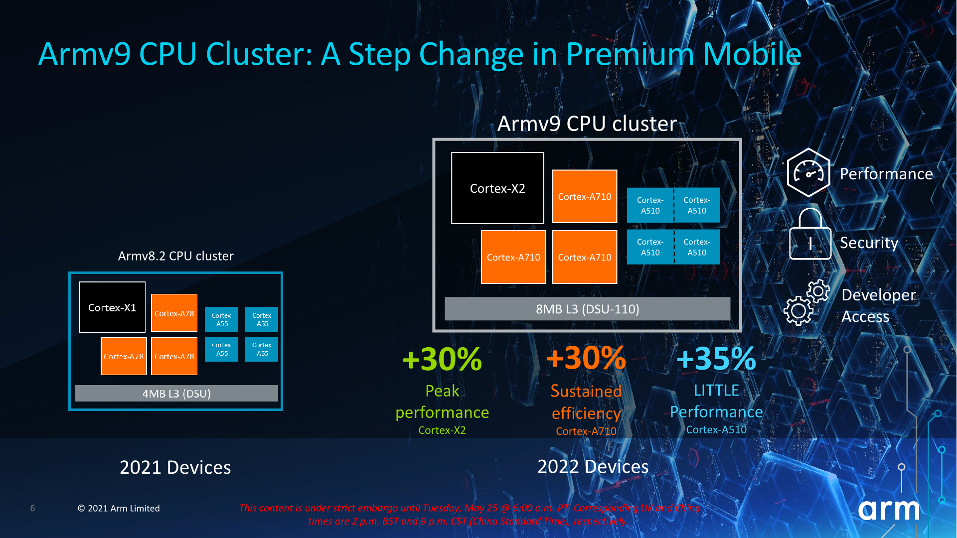
Arm has also made some more lofty performance claims when it comes to actual device implementations in 2022, such as +30% peak-to-peak performance boosts on the parts of the X2 cores. Generally, given our expectations that both the next Snapdragon and the next Exynos flagships will come in a similar Samsung foundry process node with smaller improvements, I’m very doubtful we’ll be seeing such larger generational improvements in practice, unless somehow MediaTek surprises us with a flagship X2 SoC made out at TSMC.
While the X2 and A710 aren’t all that groundbreaking, we have to note that the move towards Armv9 brings a lot of new architectural features that would otherwise eat into the expected yearly performance or efficiency improvements. The move to the new ISA baseline has been a long time coming and I’m curious to see what it will enable in terms of media applications (SVE) or AI (new ML instructions).
This is also the fourth and last iteration of Arm’s Austin core family, so hopefully next year’s new Sophia family will see larger generational leaps. Arm admits that we’re nearing diminishing returns and it’s certainly not at the same break-neck pace it was moving a few years ago, but there’s still a lot which can be done.
Today we also saw the unveiling of a brand-new little core in the form of the Cortex-A510. A new clean-sheet design from the Cambridge team, it’s certainly using an innovative approach given its “merged core” design, sharing the L2 cache hierarchy and the FP/SIMD back-end amongst two otherwise full featured cores. The performance and IPC gains are claimed to be quite large at +35-50%, however it seems that this generation hasn’t improved the efficiency curve all that much. It’s still a much better design and will have effective benefits for power efficiency in real-world workloads due to how workloads interact between the little and larger cores, but leaves us with a feeling that it doesn’t provide a knock-out convincing jump we had expected after 4 years. The silver lining here is that Arm is promising further generational improvements in performance and power with subsequent iterations, so we won’t be left with the current state of affairs the same way we saw the Cortex-A55 stagnate.
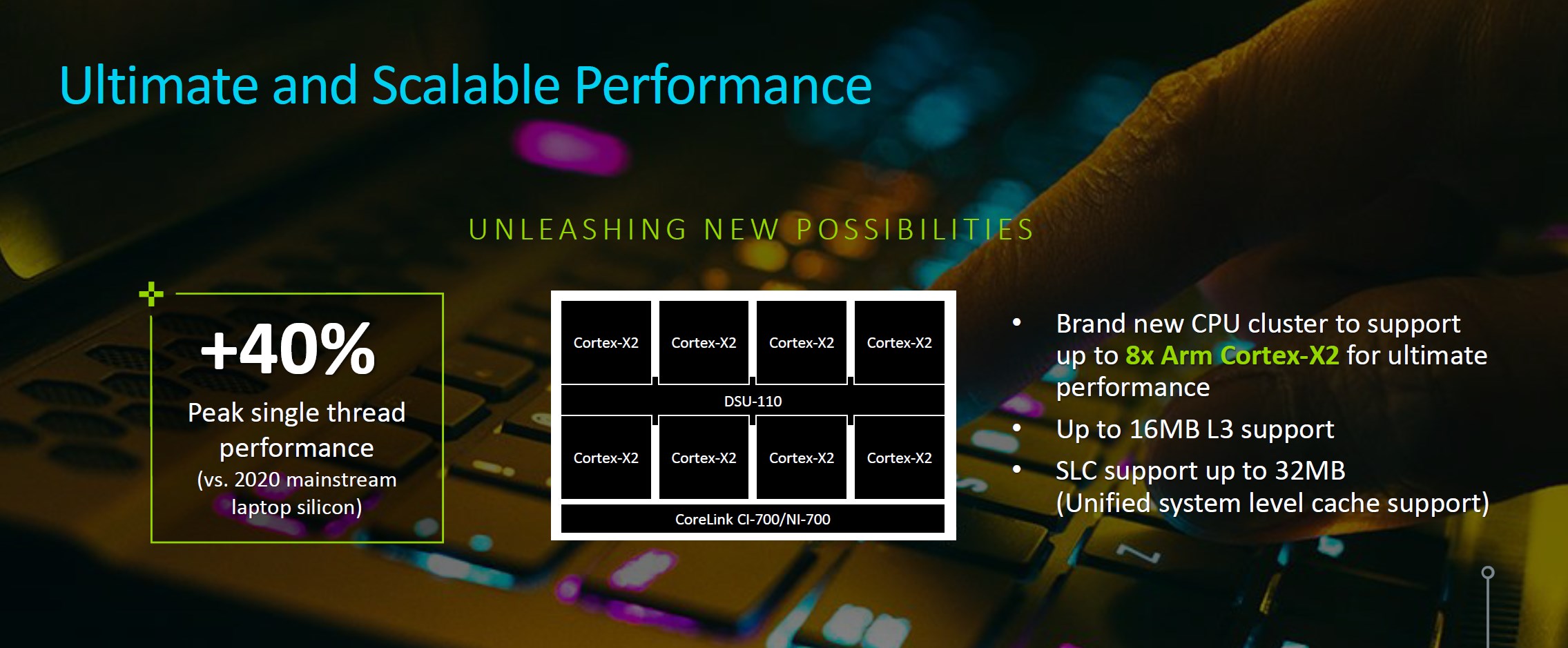
One of the more key points I saw Arm put their focus on was the new possibilities in larger form-factor devices beyond mobile. The new DSU-110 now supports up to 8 Cortex-X2 cores, a theoretical setup that would pretty much blow away the current Cortex-A76 based Arm laptop SoCs such as the Snapdragon 8cx family. The new cluster design allows for large L3 caches of up to 16MB, and while I don’t know if we’ll see the new interconnect IPs used by the larger vendors, it surely also makes a big argument for larger performance designs. The catch is that if Qualcomm were to adopt and make such a design, it would seemingly be short-lived given their recent Nuvia acquisition and intent on using custom cores. Otherwise, because of a lack of Mali Windows drivers, this really only leaves space for a theoretical Samsung laptop SoC with AMD RDNA GPU, but such a SoC could nonetheless be very successful.
Overall, this year’s CPU and system IP announcements from Arm are extremely solid new IP offerings, really laying down a new foundation, both architecturally with Armv9, and microarchitecturally thanks to elements such as the new DSU and the new little core CPUs. We’re looking forward to the new 2022 SoCs and products that will be powered by the new Arm IP.


181 Comments
View All Comments
ChrisGX - Thursday, May 27, 2021 - link
Using Andrei's initial performance estimate for the X1 (clocked at 3GHz) as a guide (47.2 SPECint2006) and ARM's own projection for the peak performance boost offered by the X2 over the X1 (+30% when process optimisations and frequency increases are factored in) we get a rating of 61.4 SPECint2006 for next years X series core. That is really a best case estimate and it is where the good news ends.The information we have on the 2022 Cortex cores does seem to lack the transparency of material of this sort that had been issued in earlier years by ARM. It is disappointing not to have any core frequency data in that information. A lot turns on realistic estimations of attainable core frequencies and having a good sense of power dissipation at maximum burst frequencies. We now know that Andrei's performance estimate for the X1 core wasn't borne out in practice (the actual performance exhibited by the highest performing X1 core - the one in the Snapdragon 888 - was 14% lower at 41.3 SPECint2006) owing to pitiful power dissipation characteristics of Samsung's 5nm LPE process that in order to prevent thermal build up and keep power consumption within budget on SoCs incorporating an X1 core SoC designers found it necessary to either a) reduce burst clock frequencies to below 3GHz or b) use restrictive power management controls to damp down chip operations threatening the thermal stability of the SoC that will naturally have the effect of throttling performance.
Using more realistic assumptions to project the likely performance of the X2 core (which I suspect might still be too optimistic because these forthcoming SoCs that incorporate an X2 core like the flagship Android smartphone SoCs of 2021 are said to be scheduled for production on Samsung fabs which must cast a degree of doubt on ARM's performance projections because recently Samsung's silicon process technologies have demonstrably failed to come up tp ARM's expectations) we get this number: 53.7 SPECint2006 (which represents the actual performance of the highest performing X1 core of 2021 x 1.3). Given the lack of transparency in the ARM data it is possible to entertain a rather broad range of imaginable SPEC peak integer performance ratings for the X2 core. A SPECspeed of 53.7 is my best guess.
ikjadoon - Tuesday, May 25, 2021 - link
These are geometric means of integer & FP scores. Typo for X1, ~50 not ~40. Let's be precise, now that I'm not on a phone ;)SPEC2006 1T Geomean:
A14 Firestorm = 71.72 points
A13 Lightning = 59.09 points
SD888 X1 = 49.48 points
Awarding the X2 the full 16% jump on both integer & FP, we can napkin math this to a Reference X2 = 57.40 at iso-frequency.
You're right they can (and maybe should) boost clocks so it could surpass the A13, but it's unrealistic to imagine Qualcomm shipping a 3.3+ GHz smartphone in 2022, especially if it's Samsung foundries again, but even on TSMC. Qualcomm's SD888 X1 at 2.84 GHz already ate 9621 joules (SPECint2006) and 4972 joules (SPECfp2006).
From https://www.anandtech.com/show/16463/snapdragon-88...
No one expects a literal doubling, but Arm's competition (NUVIA, Apple, Ampere) are not slowing down, either.
Wilco1 - Tuesday, May 25, 2021 - link
OK I get it now - the 40 made me think you meant SPECINT as that is what Cortex-X1 scored.3.3GHz on TSMC 5nm is conservative given it has significant performance/power improvements (which the A14 already benefits from), but yes it means switching back to TSMC.
Thala - Tuesday, May 25, 2021 - link
Indeed the performance gains of A14 vs. A13 are mostly frequency driven and much less IPC driven. It is not unreasonable to assume some frequency gains for X2 as well when moving to 5nm TSMC.Ppietra - Wednesday, May 26, 2021 - link
Thala, looking at the numbers IPC improved 8%, being responsible for 42% of performance growth... so not exactly much less!A13 to A14 transition gives no clue about what would happen between X1 and X2 or between Samsung and TSMC... X1 is already at 5nm, and its clock speed is just 5% less than the A14... Their designs priorities are also different, so you cannot infer much!
name99 - Tuesday, May 25, 2021 - link
All true. But of course A14 is an especially easy opponent!- it's the last round of what appears to be Apple's 4-year "seriously new micro-architecture" cadence -- A77..A10 as gen 1, A11..A14 as gen 2, A15 et seq as gen 3.
- it was clearly designed with the single highest priority being get the x86 stuff working. Meaning that anything that did not match that priority (including, eg, optimized physical layout and risky micro-architectural innovations) was punted till the A15
- it doesn't have SVE/2, which is good for anything up to a 80% speed boost depending on the exact code (even with just compiler vectorization). Averaging over "representative code bases" is a game that's never going to get everyone to agree, but the one attempt I saw to do this came up with an average performance boost of ~30%.
Given how *low* ARM's numbers are, I assume they're talking about performance in the absence of use of SVE/2? Honestly the whole thing is kinda weird, how little they're pushing the SVE/2 angle and how much one might expect it to improve things.
I do *not* expect Apple to be as timid... And while Apple tend to shy away from hardware announcements at WWDC, we all know about M1 by now, AND we know that SVE/2 will be in next year's ARM (so presumably in this year's Apple). Meaning maybe there will be some talks about SVE/2 (and other ARMv9 stuff) at WWDC?
Wilco1 - Tuesday, May 25, 2021 - link
You are exaggerating the gains of SIMD in general. Yes automatic vectorization helps, but even if it improves some image transformations by 80%, it's never going to speed up browsing by 30%. Or any other general purpose code. Or SPEC.Remember this is 128-bit SVE, so 4 Neon units are about as fast as 4 SVE units. For great SVE performance on HPC code look at A64FX or the upcoming Neoverse V1.
name99 - Tuesday, May 25, 2021 - link
- One hopes that the combination of agnostic length and predicates will allow a lot of code for which vectorization was previously uneconomical (too expensive to mask out fiddly bits, too much overhead in loop prologs and epilogs) to now be handled. We shall see.- You are right about the 128b of course; yet another instance of ARM never trying for a stretch goal! I assume Apple will be implementing this as 2x256, meaning, among other things, the path from L1D to LSU grows from 128b to 256b wide, and that's an example of where SVE/2 (indirectly, sure) helps boost performance for everyone.
smalM - Friday, May 28, 2021 - link
Could you please explain why you asume Apple will reduce the number of FP/SIMD units in exchange for widening them. Is that really better? From a FP or from a SIMD standpoint?Thanks in advance.
Making the path from L1D to LSU 256b wide is something Apple could do anyways and is not directly related to SVE2; I was astonished they didn't do it when they added the fourth FP/NEON unit.
mode_13h - Saturday, May 29, 2021 - link
> would you please explain why you asume Apple will reduce the number of FP/SIMD units> in exchange for widening them. Is that really better?
For SVE it's a little better, since it means software having to run loops for about half as many iterations, correspondingly reducing loop overhead.
> Making the path from L1D to LSU 256b wide is something Apple could
> do anyways and is not directly related to SVE2
I don't really see why. It seems like it'd only help for back-to-back reads or writes from/to consecutive addresses. And if 128-bits is already enough to do that, then extra width would be a waste.