Arm Announces Mobile Armv9 CPU Microarchitectures: Cortex-X2, Cortex-A710 & Cortex-A510
by Andrei Frumusanu on May 25, 2021 9:00 AM EST- Posted in
- SoCs
- CPUs
- Arm
- Smartphones
- Mobile
- Cortex
- ARMv9
- Cortex-X2
- Cortex-A710
- Cortex-A510
A new CI-700 Coherent Interconnect & NI-700 NoC For SoCs
Finally, the last new announcement of the day is a new interconnect and network-on-chip generation. The last time Arm had announced a mobile/client interconnect was back in in 2015 with the CCI-550. The reason for the large gap between IPs, in Arm’s own words, is that ever since Arm’s introduction of the DSU in its CPU complexes, there really hasn’t been any need for a cache coherent interconnect in the market. While that’s eyebrow-raising from a GPU perspective, it makes perfect sense from a CPU perspective, as coherency between CPU cores was the primary driver for such interconnects until then.
With the advent of new more complex computing platforms, such as NPUs, accelerators, and hopeful more use of GPUs in cache-coherent fashions, Arm saw a need gap in its portfolio and decided to update its client-side interconnect IP.
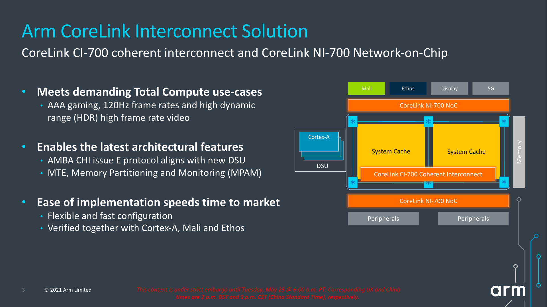
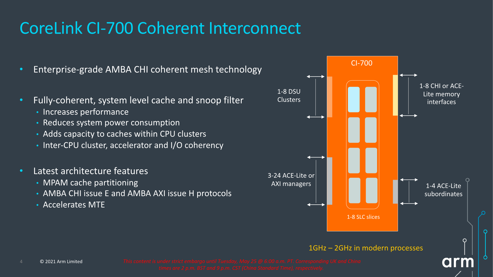
The new CI-700 is a mobile and client optimised variant of Arm’s infrastructure CMN mesh network, implementing important new interoperability with the new IP announced today, such as the new DSU or CPU cores.
The new mesh interconnect scales up from 1 to 8 DSU clusters, and supports up to 8 memory controllers, and also introduces innovations such as a system level cache.
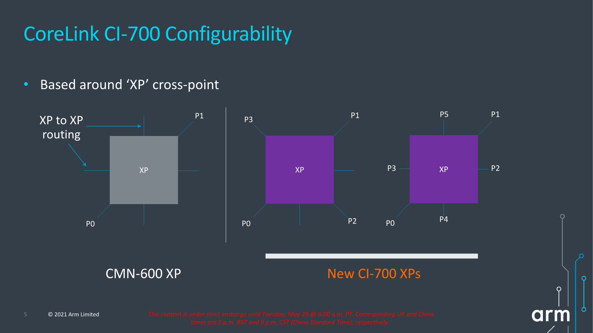
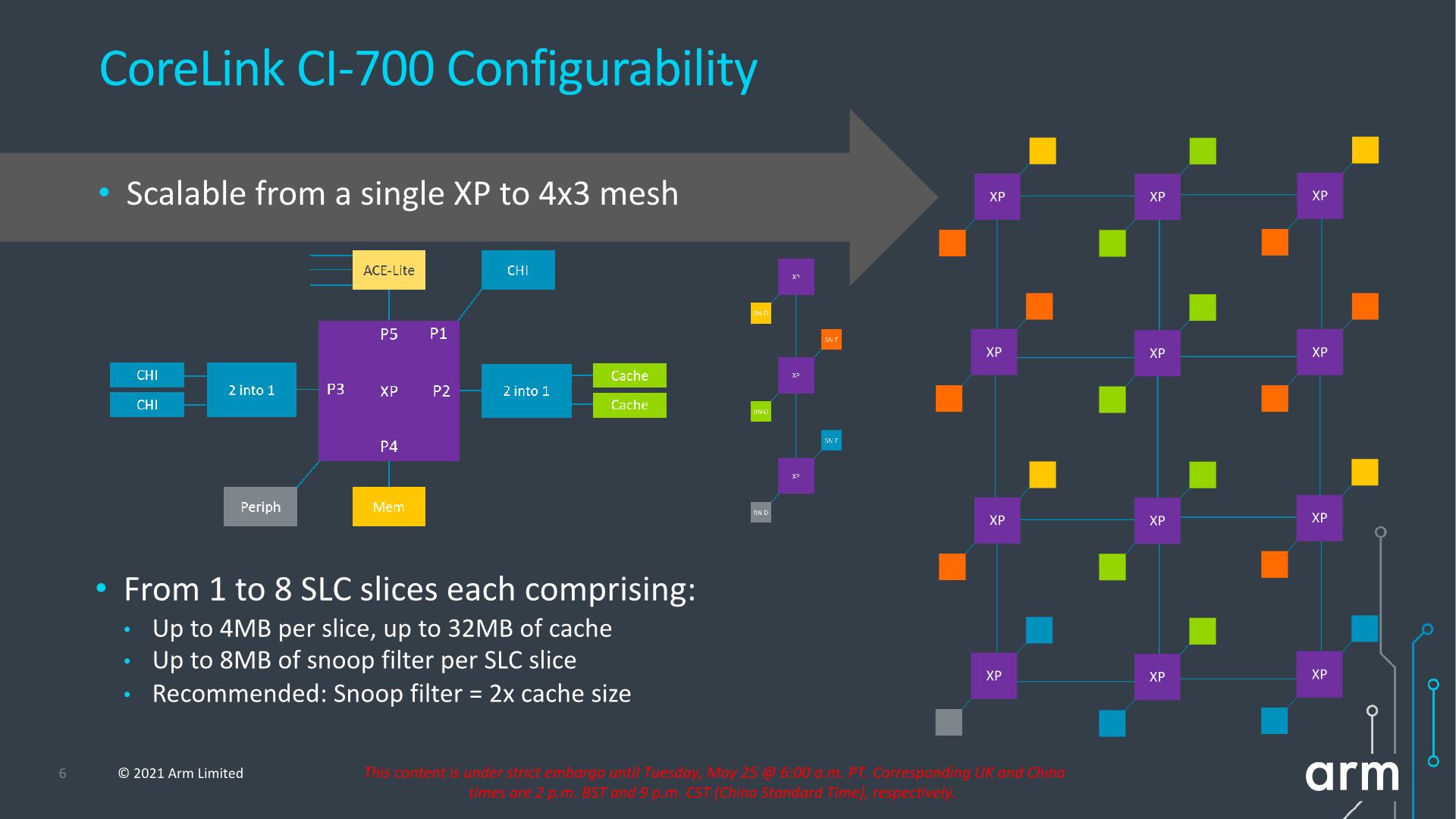
The mesh network topology and building blocks is very similar to what we’ve seen in the CMN infrastructure IP, in that “points” in the mesh are comprised of “cross-points” or “XP”. One differentiation that’s unique to the client mesh implementation is that XPs can have more attached connectivity ports, trading in routing connection paths. The new IP can also be configured as just a sole XP with no real mesh so to speak of, or essentially a 1x1 mesh configuration. This can grow up to a 4x3 mesh in the largest possible configuration.
The mesh supports from 1 to 8 SLC slices, with up to 4MB per slice for a total of 32MB, and snoop filter SRAM with coverage of up to 8MB address space per slice. It’s noted that generally Arm recommends 1.5-2x of coverage of the underlying private cache hierarchies of the mesh clients.
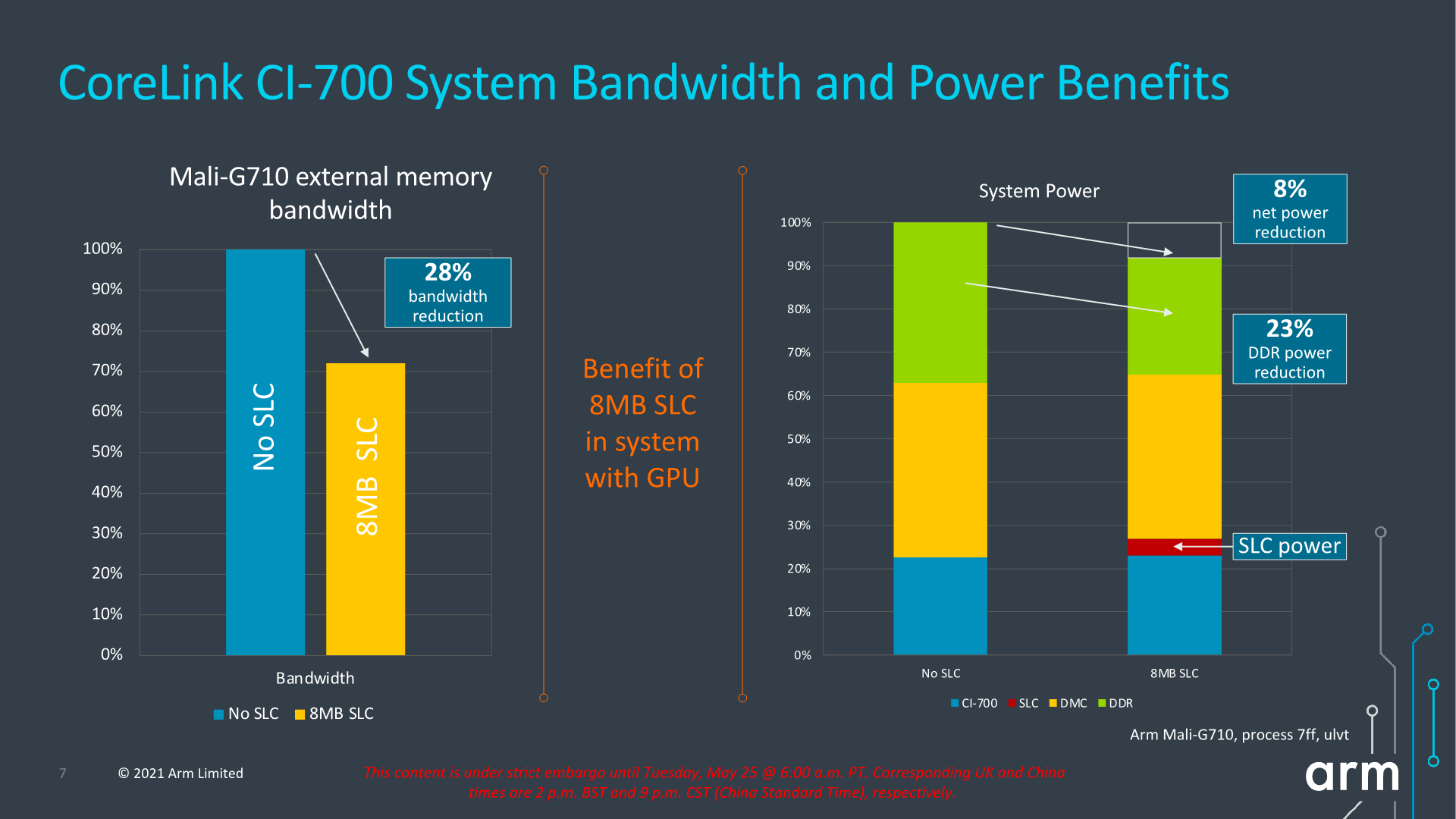
The SLC can server as both a bandwidth amplifier as well as reducing external memory/DRAM transactions, reducing system power reduction.
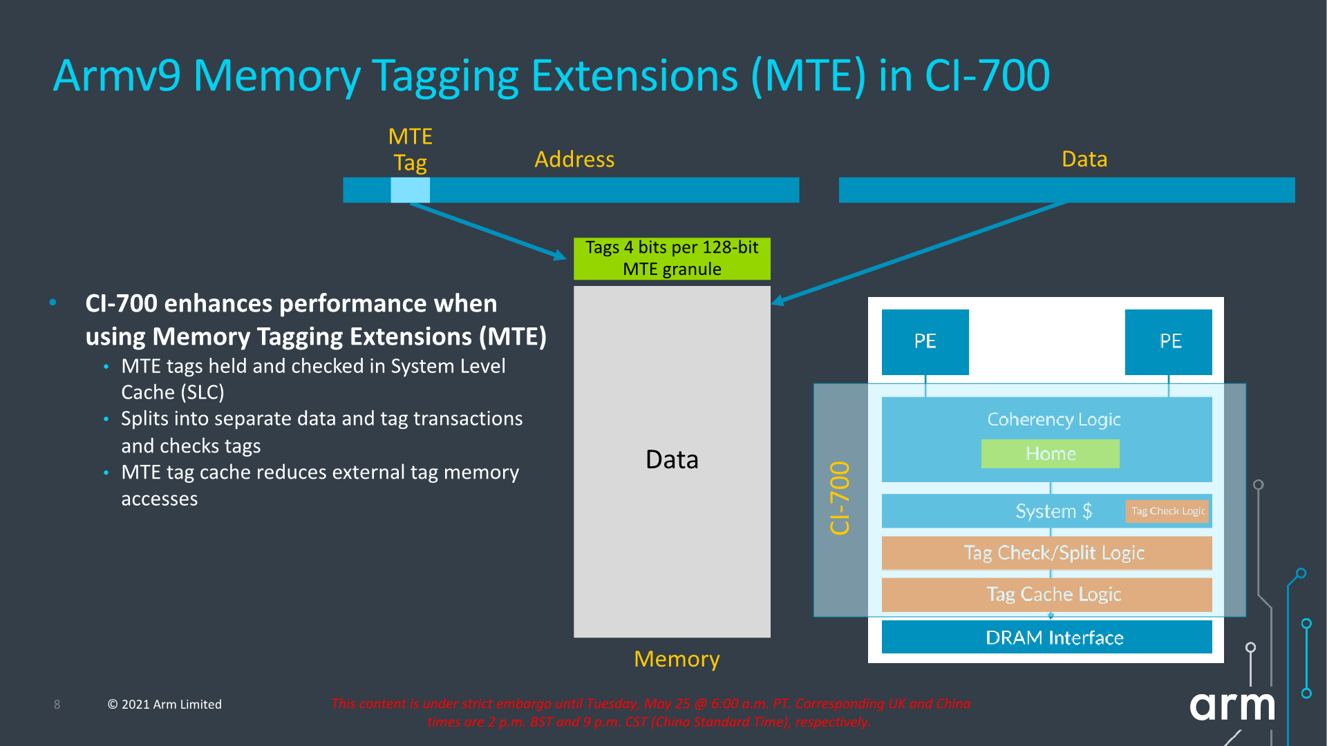
We see a reiteration of the support for MTE, allowing for this generation of IPs to support the feature across the new CPU IP, the DSU, and the new cache coherent interconnect.
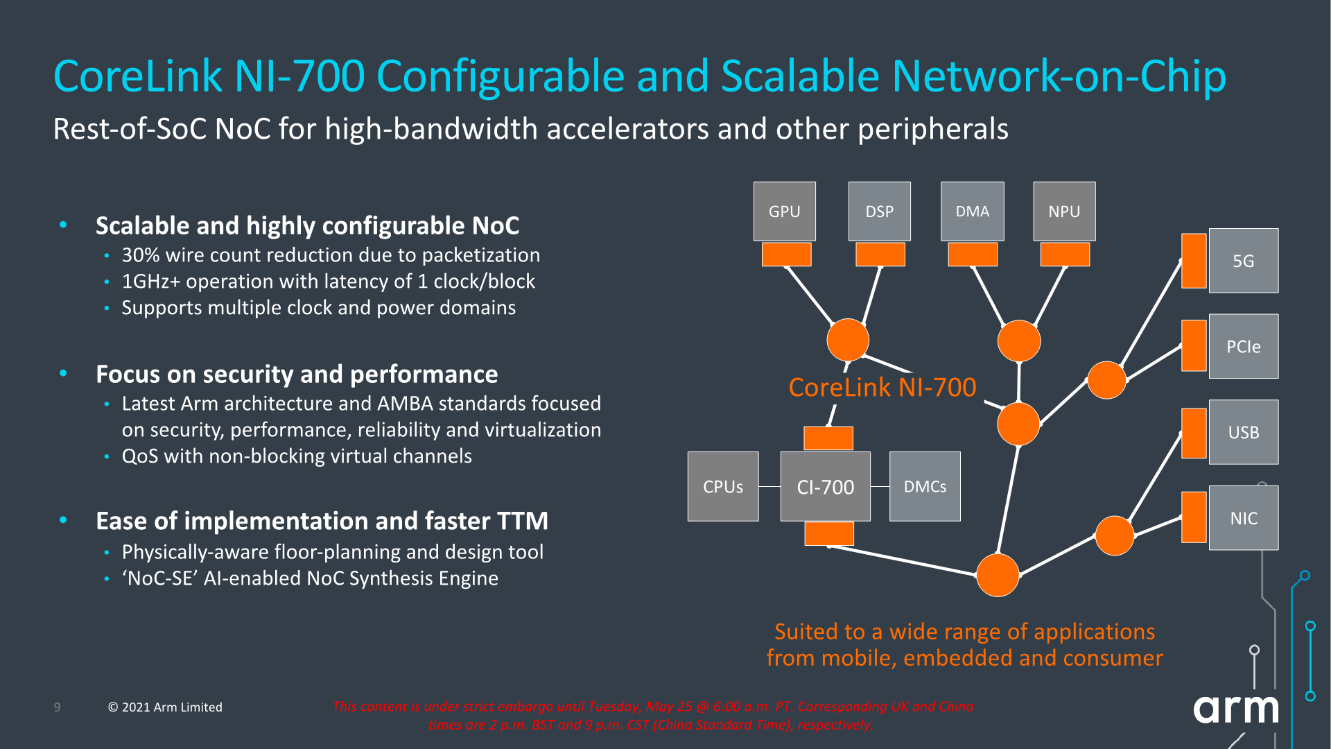
Alongside the new CI-700 coherent interconnect, we’re also seeing a new NI-700 network-on-chip for non-coherent data transfers between a SoC’s various IP blocks. The big new improvements here is the introduction of packetization for data transfers, which leads to a reduction of wires and thus improves area efficiency of the NoC on the SoC.
Overall, the new system IP announced today is very interesting, but the one question that’s one has to ask oneself is exactly who these net interconnects are meant for. Over the last few years, we’ve seen essentially every major mobile vendor roll out their own in-house cache-coherent interconnect IP, such as Samsung’s SCI or MediaTek’s MCSI, and other times we don’t see vendors talk about their in-house interconnects at all (Qualcomm). Due to almost everybody having their own IP, I’m not sure what the likelihood would be that any of the big players would jump back to Arm’s own solutions – if somebody were to adopt it, it would rather be amongst the smaller name vendors and newcomers to the market. From a business and IP portfolio perspective, the new designs make a lot of sense and allows to have the building blocks to create a mostly Arm-only SoC, which is an important item to have on the menu for Arm’s more diverse customer base.


181 Comments
View All Comments
ChrisGX - Thursday, May 27, 2021 - link
Using Andrei's initial performance estimate for the X1 (clocked at 3GHz) as a guide (47.2 SPECint2006) and ARM's own projection for the peak performance boost offered by the X2 over the X1 (+30% when process optimisations and frequency increases are factored in) we get a rating of 61.4 SPECint2006 for next years X series core. That is really a best case estimate and it is where the good news ends.The information we have on the 2022 Cortex cores does seem to lack the transparency of material of this sort that had been issued in earlier years by ARM. It is disappointing not to have any core frequency data in that information. A lot turns on realistic estimations of attainable core frequencies and having a good sense of power dissipation at maximum burst frequencies. We now know that Andrei's performance estimate for the X1 core wasn't borne out in practice (the actual performance exhibited by the highest performing X1 core - the one in the Snapdragon 888 - was 14% lower at 41.3 SPECint2006) owing to pitiful power dissipation characteristics of Samsung's 5nm LPE process that in order to prevent thermal build up and keep power consumption within budget on SoCs incorporating an X1 core SoC designers found it necessary to either a) reduce burst clock frequencies to below 3GHz or b) use restrictive power management controls to damp down chip operations threatening the thermal stability of the SoC that will naturally have the effect of throttling performance.
Using more realistic assumptions to project the likely performance of the X2 core (which I suspect might still be too optimistic because these forthcoming SoCs that incorporate an X2 core like the flagship Android smartphone SoCs of 2021 are said to be scheduled for production on Samsung fabs which must cast a degree of doubt on ARM's performance projections because recently Samsung's silicon process technologies have demonstrably failed to come up tp ARM's expectations) we get this number: 53.7 SPECint2006 (which represents the actual performance of the highest performing X1 core of 2021 x 1.3). Given the lack of transparency in the ARM data it is possible to entertain a rather broad range of imaginable SPEC peak integer performance ratings for the X2 core. A SPECspeed of 53.7 is my best guess.
ikjadoon - Tuesday, May 25, 2021 - link
These are geometric means of integer & FP scores. Typo for X1, ~50 not ~40. Let's be precise, now that I'm not on a phone ;)SPEC2006 1T Geomean:
A14 Firestorm = 71.72 points
A13 Lightning = 59.09 points
SD888 X1 = 49.48 points
Awarding the X2 the full 16% jump on both integer & FP, we can napkin math this to a Reference X2 = 57.40 at iso-frequency.
You're right they can (and maybe should) boost clocks so it could surpass the A13, but it's unrealistic to imagine Qualcomm shipping a 3.3+ GHz smartphone in 2022, especially if it's Samsung foundries again, but even on TSMC. Qualcomm's SD888 X1 at 2.84 GHz already ate 9621 joules (SPECint2006) and 4972 joules (SPECfp2006).
From https://www.anandtech.com/show/16463/snapdragon-88...
No one expects a literal doubling, but Arm's competition (NUVIA, Apple, Ampere) are not slowing down, either.
Wilco1 - Tuesday, May 25, 2021 - link
OK I get it now - the 40 made me think you meant SPECINT as that is what Cortex-X1 scored.3.3GHz on TSMC 5nm is conservative given it has significant performance/power improvements (which the A14 already benefits from), but yes it means switching back to TSMC.
Thala - Tuesday, May 25, 2021 - link
Indeed the performance gains of A14 vs. A13 are mostly frequency driven and much less IPC driven. It is not unreasonable to assume some frequency gains for X2 as well when moving to 5nm TSMC.Ppietra - Wednesday, May 26, 2021 - link
Thala, looking at the numbers IPC improved 8%, being responsible for 42% of performance growth... so not exactly much less!A13 to A14 transition gives no clue about what would happen between X1 and X2 or between Samsung and TSMC... X1 is already at 5nm, and its clock speed is just 5% less than the A14... Their designs priorities are also different, so you cannot infer much!
name99 - Tuesday, May 25, 2021 - link
All true. But of course A14 is an especially easy opponent!- it's the last round of what appears to be Apple's 4-year "seriously new micro-architecture" cadence -- A77..A10 as gen 1, A11..A14 as gen 2, A15 et seq as gen 3.
- it was clearly designed with the single highest priority being get the x86 stuff working. Meaning that anything that did not match that priority (including, eg, optimized physical layout and risky micro-architectural innovations) was punted till the A15
- it doesn't have SVE/2, which is good for anything up to a 80% speed boost depending on the exact code (even with just compiler vectorization). Averaging over "representative code bases" is a game that's never going to get everyone to agree, but the one attempt I saw to do this came up with an average performance boost of ~30%.
Given how *low* ARM's numbers are, I assume they're talking about performance in the absence of use of SVE/2? Honestly the whole thing is kinda weird, how little they're pushing the SVE/2 angle and how much one might expect it to improve things.
I do *not* expect Apple to be as timid... And while Apple tend to shy away from hardware announcements at WWDC, we all know about M1 by now, AND we know that SVE/2 will be in next year's ARM (so presumably in this year's Apple). Meaning maybe there will be some talks about SVE/2 (and other ARMv9 stuff) at WWDC?
Wilco1 - Tuesday, May 25, 2021 - link
You are exaggerating the gains of SIMD in general. Yes automatic vectorization helps, but even if it improves some image transformations by 80%, it's never going to speed up browsing by 30%. Or any other general purpose code. Or SPEC.Remember this is 128-bit SVE, so 4 Neon units are about as fast as 4 SVE units. For great SVE performance on HPC code look at A64FX or the upcoming Neoverse V1.
name99 - Tuesday, May 25, 2021 - link
- One hopes that the combination of agnostic length and predicates will allow a lot of code for which vectorization was previously uneconomical (too expensive to mask out fiddly bits, too much overhead in loop prologs and epilogs) to now be handled. We shall see.- You are right about the 128b of course; yet another instance of ARM never trying for a stretch goal! I assume Apple will be implementing this as 2x256, meaning, among other things, the path from L1D to LSU grows from 128b to 256b wide, and that's an example of where SVE/2 (indirectly, sure) helps boost performance for everyone.
smalM - Friday, May 28, 2021 - link
Could you please explain why you asume Apple will reduce the number of FP/SIMD units in exchange for widening them. Is that really better? From a FP or from a SIMD standpoint?Thanks in advance.
Making the path from L1D to LSU 256b wide is something Apple could do anyways and is not directly related to SVE2; I was astonished they didn't do it when they added the fourth FP/NEON unit.
mode_13h - Saturday, May 29, 2021 - link
> would you please explain why you asume Apple will reduce the number of FP/SIMD units> in exchange for widening them. Is that really better?
For SVE it's a little better, since it means software having to run loops for about half as many iterations, correspondingly reducing loop overhead.
> Making the path from L1D to LSU 256b wide is something Apple could
> do anyways and is not directly related to SVE2
I don't really see why. It seems like it'd only help for back-to-back reads or writes from/to consecutive addresses. And if 128-bits is already enough to do that, then extra width would be a waste.