Arm Announces Mobile Armv9 CPU Microarchitectures: Cortex-X2, Cortex-A710 & Cortex-A510
by Andrei Frumusanu on May 25, 2021 9:00 AM EST- Posted in
- SoCs
- CPUs
- Arm
- Smartphones
- Mobile
- Cortex
- ARMv9
- Cortex-X2
- Cortex-A710
- Cortex-A510
New DSU-110 L3 & Cluster: Massively More Bandwidth
Alongside the new CPU microarchitectures, Arm today is also announcing a new L3 design in the form of the new DSU-110. The “DynamIQ Shared Unit” had been the company’s go-to cluster and “core complex” block ever since it was introduced in 2017 with the Cortex-A75 and Cortex-A55. While we’ve seen small iterative improvements, today’s DSU-110 marks a major change in how the DSU operates and how it promises to scale up in cache size and bandwidth.
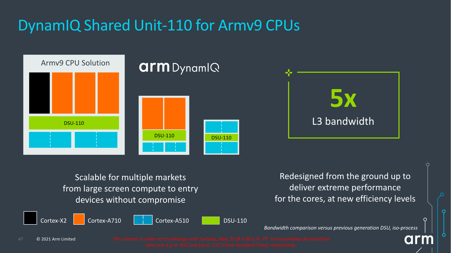
The new DSU-110 is a ground-up redesign with an emphasis on more bandwidth and more power efficiency. It continues to be the core building block for all of Arm’s mobile and lower tier market segments.
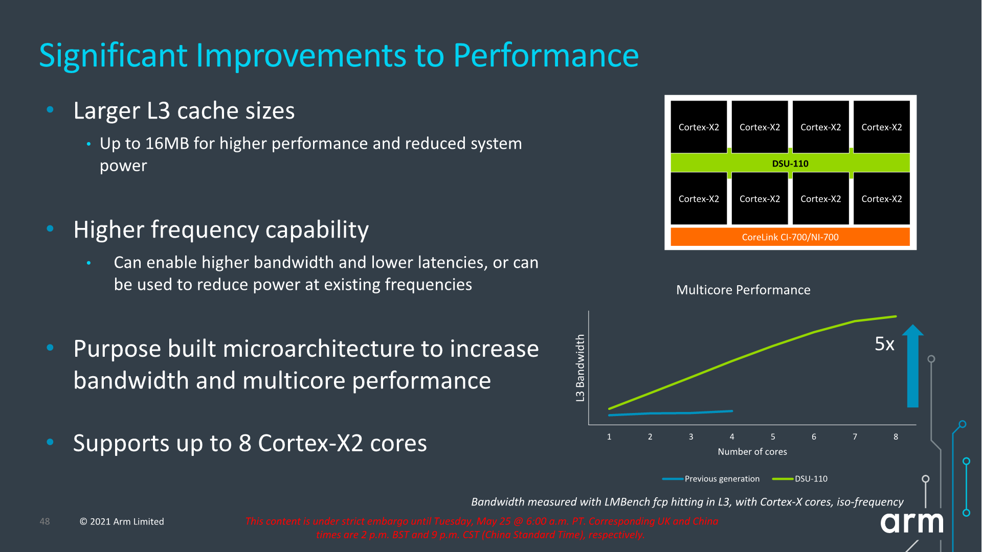
A key metric is of course the increase of L3 cache configuration which will now go up to 16MB this generation. This is of course the high-end of the spectrum and generally we shouldn’t expect such a configuration in a mobile SoC soon, but Arm has had several slides depicting larger form-factor implementations using such a larger design housing up to 8 Cortex-X2 cores. This is undoubtedly extremely interesting for a higher-performance laptop use-case.
The bandwidth increase of the new design is also significant, and applies from single-thread to multi-threaded scenarios. The new DSU-110 promises aggregate bandwidth increases of up to 5x compared to the contemporary design. More interesting is the fact that it also significantly boosts single-core bandwidth, and Arm here actually notes that the new DSU can actually support more bandwidth than what’s actually capable of the new core microarchitectures for the time being.
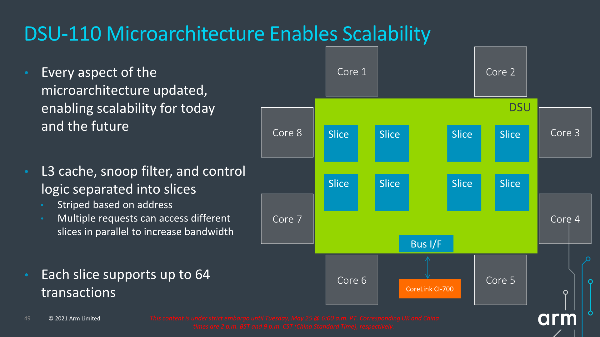
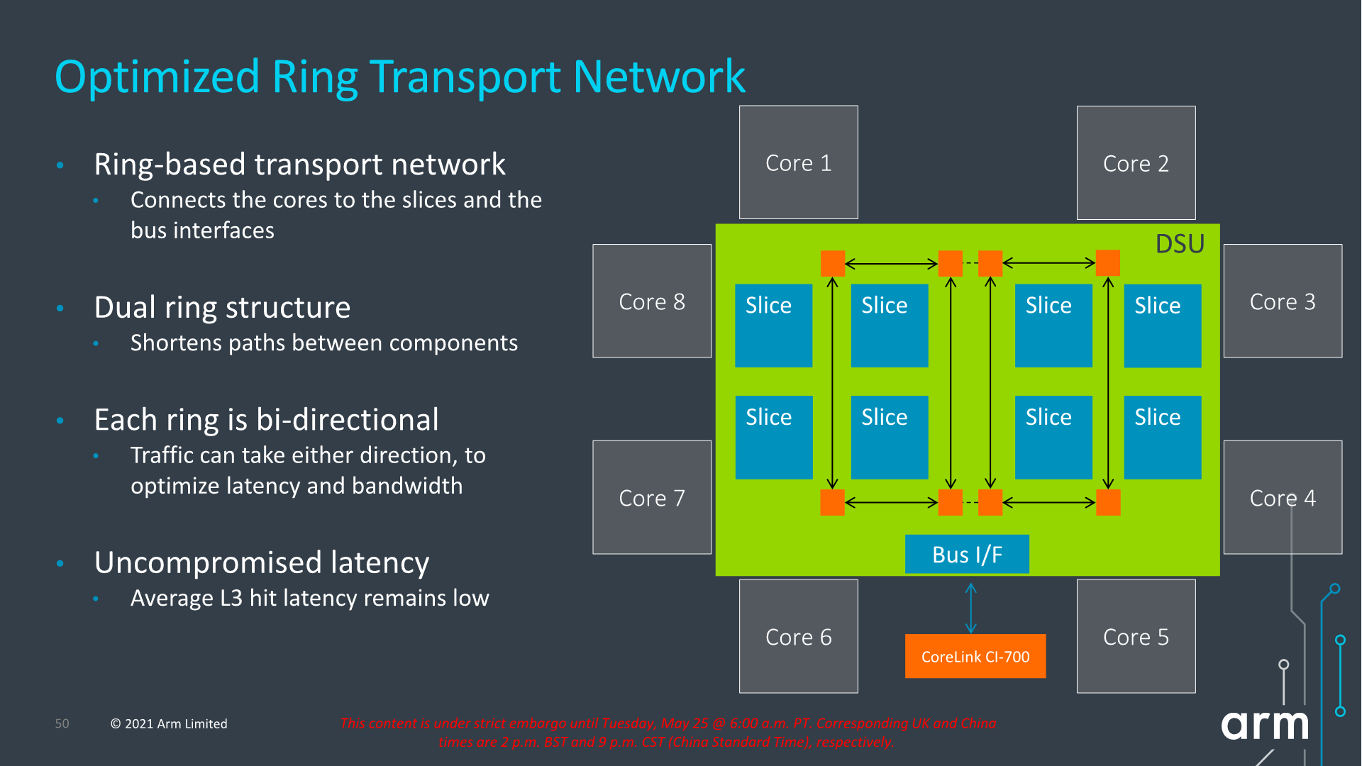
Arm never really disclosed the internal topology of the previous generation DSU, but remarks that with the DSU-110 the company has shifted over to a bi-directional dual-ring transport topology, each with four ring-stops, and now supporting up to 8 cache slices. The dual-ring structure is used to reduce the latencies and hops between ring-stops and in shorten the paths between the cache slices and cores. Arm notes that they’ve tried to retain the same lower access latencies as on the current generation DSU (cache size increases aside), so we should be seeing very similar average latencies between the two generations.
Parallel access increases for bandwidth as well as more outstanding transactions seem to have been also very important in order to improve performance, which seems very exciting for upcoming SoC designs, but also puts into more question the previously presented CPU IPC improvements and exactly how much the new DSU-110 contributes to those numbers.
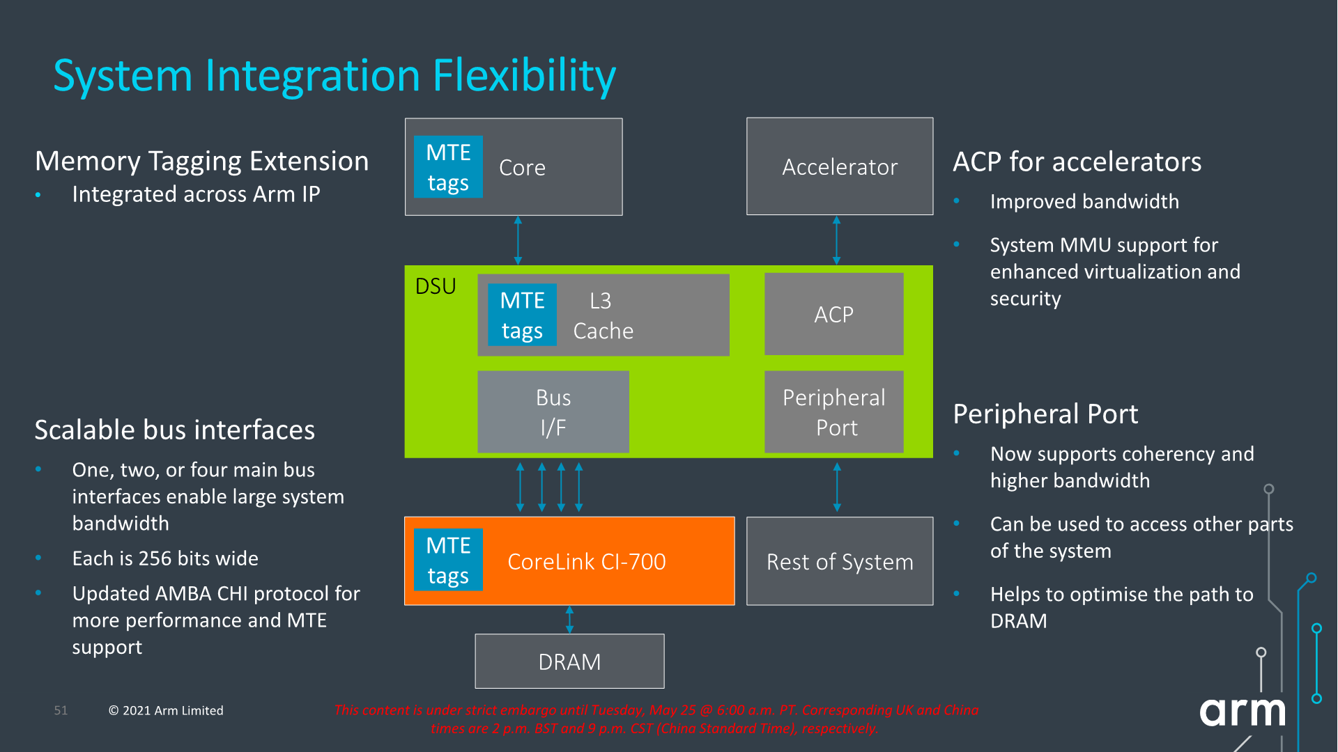
Architecturally, one important change to the capabilities of the DSU-110 is support for MTE tags, a upcoming security and debugging feature promising to greatly help with memory safety issues.
The new DSU can scale up to 4x AMBA CHI ports, meaning we’ll have up to 1024-bit total bi-directional bandwidth to the system memory. With a theoretical DSU clock of around 2GHz this would enable bandwidth of up to 256GB/s reads or writes, or double that when combined, plenty enough to be able to saturate also eventual high-end laptop configurations.

In terms of power efficiency, the new DSU offers more options for low-power operation when in idle situations, implementing partial L3 power-down, able to reduce leakage power of up to 75% compared to the current DSU.
In general idle situations but still having the full L3 powered on, the new design promises up to 25% reduction in leakage power all whilst offering 2x the bandwidth capabilities.
It’s important to note that we’re talking about leakage power here- active dynamic power is expected to generally scale linearly with the bandwidth increase of the new design, meaning 5x the bandwidth would also cost 5x the power. This would be an important factor to note into system power and in general the expected power behaviour of the next-gen SoCs when they’re put under heavy memory workloads.
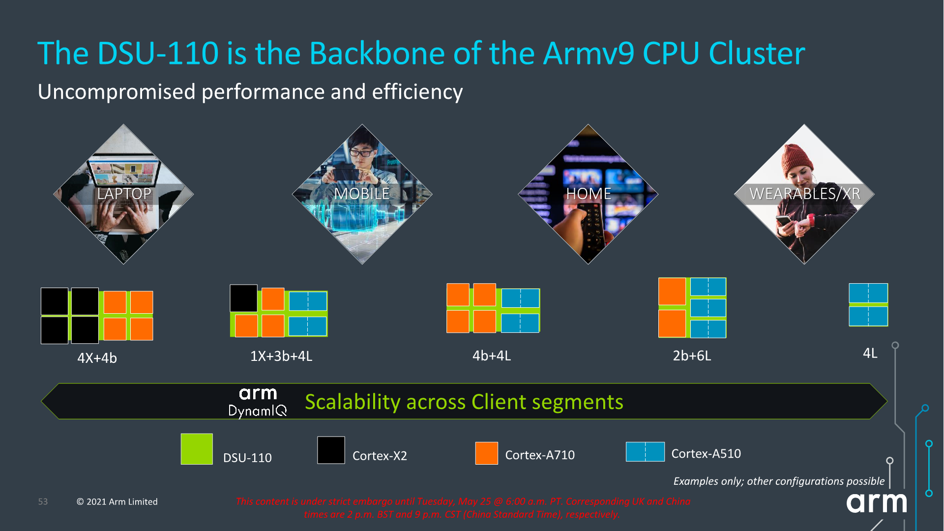
Arm describes the DSU-110 as the backbone of the Armv9 cluster and that seemingly seems to be an apt description. The new bandwidth capabilities are sure to help out both with single-threaded, but also with multi-threaded performance of upcoming SoCs. Generally, the new 16MB L3 capability, while it’s possible somebody might do a high-end laptop SoC configuration, isn’t as exciting as the now finally expected move to a new 8MB L3 on mobile SoCs, hopefully also enabling higher power efficiency and more battery life for devices.


181 Comments
View All Comments
ChrisGX - Thursday, May 27, 2021 - link
Using Andrei's initial performance estimate for the X1 (clocked at 3GHz) as a guide (47.2 SPECint2006) and ARM's own projection for the peak performance boost offered by the X2 over the X1 (+30% when process optimisations and frequency increases are factored in) we get a rating of 61.4 SPECint2006 for next years X series core. That is really a best case estimate and it is where the good news ends.The information we have on the 2022 Cortex cores does seem to lack the transparency of material of this sort that had been issued in earlier years by ARM. It is disappointing not to have any core frequency data in that information. A lot turns on realistic estimations of attainable core frequencies and having a good sense of power dissipation at maximum burst frequencies. We now know that Andrei's performance estimate for the X1 core wasn't borne out in practice (the actual performance exhibited by the highest performing X1 core - the one in the Snapdragon 888 - was 14% lower at 41.3 SPECint2006) owing to pitiful power dissipation characteristics of Samsung's 5nm LPE process that in order to prevent thermal build up and keep power consumption within budget on SoCs incorporating an X1 core SoC designers found it necessary to either a) reduce burst clock frequencies to below 3GHz or b) use restrictive power management controls to damp down chip operations threatening the thermal stability of the SoC that will naturally have the effect of throttling performance.
Using more realistic assumptions to project the likely performance of the X2 core (which I suspect might still be too optimistic because these forthcoming SoCs that incorporate an X2 core like the flagship Android smartphone SoCs of 2021 are said to be scheduled for production on Samsung fabs which must cast a degree of doubt on ARM's performance projections because recently Samsung's silicon process technologies have demonstrably failed to come up tp ARM's expectations) we get this number: 53.7 SPECint2006 (which represents the actual performance of the highest performing X1 core of 2021 x 1.3). Given the lack of transparency in the ARM data it is possible to entertain a rather broad range of imaginable SPEC peak integer performance ratings for the X2 core. A SPECspeed of 53.7 is my best guess.
ikjadoon - Tuesday, May 25, 2021 - link
These are geometric means of integer & FP scores. Typo for X1, ~50 not ~40. Let's be precise, now that I'm not on a phone ;)SPEC2006 1T Geomean:
A14 Firestorm = 71.72 points
A13 Lightning = 59.09 points
SD888 X1 = 49.48 points
Awarding the X2 the full 16% jump on both integer & FP, we can napkin math this to a Reference X2 = 57.40 at iso-frequency.
You're right they can (and maybe should) boost clocks so it could surpass the A13, but it's unrealistic to imagine Qualcomm shipping a 3.3+ GHz smartphone in 2022, especially if it's Samsung foundries again, but even on TSMC. Qualcomm's SD888 X1 at 2.84 GHz already ate 9621 joules (SPECint2006) and 4972 joules (SPECfp2006).
From https://www.anandtech.com/show/16463/snapdragon-88...
No one expects a literal doubling, but Arm's competition (NUVIA, Apple, Ampere) are not slowing down, either.
Wilco1 - Tuesday, May 25, 2021 - link
OK I get it now - the 40 made me think you meant SPECINT as that is what Cortex-X1 scored.3.3GHz on TSMC 5nm is conservative given it has significant performance/power improvements (which the A14 already benefits from), but yes it means switching back to TSMC.
Thala - Tuesday, May 25, 2021 - link
Indeed the performance gains of A14 vs. A13 are mostly frequency driven and much less IPC driven. It is not unreasonable to assume some frequency gains for X2 as well when moving to 5nm TSMC.Ppietra - Wednesday, May 26, 2021 - link
Thala, looking at the numbers IPC improved 8%, being responsible for 42% of performance growth... so not exactly much less!A13 to A14 transition gives no clue about what would happen between X1 and X2 or between Samsung and TSMC... X1 is already at 5nm, and its clock speed is just 5% less than the A14... Their designs priorities are also different, so you cannot infer much!
name99 - Tuesday, May 25, 2021 - link
All true. But of course A14 is an especially easy opponent!- it's the last round of what appears to be Apple's 4-year "seriously new micro-architecture" cadence -- A77..A10 as gen 1, A11..A14 as gen 2, A15 et seq as gen 3.
- it was clearly designed with the single highest priority being get the x86 stuff working. Meaning that anything that did not match that priority (including, eg, optimized physical layout and risky micro-architectural innovations) was punted till the A15
- it doesn't have SVE/2, which is good for anything up to a 80% speed boost depending on the exact code (even with just compiler vectorization). Averaging over "representative code bases" is a game that's never going to get everyone to agree, but the one attempt I saw to do this came up with an average performance boost of ~30%.
Given how *low* ARM's numbers are, I assume they're talking about performance in the absence of use of SVE/2? Honestly the whole thing is kinda weird, how little they're pushing the SVE/2 angle and how much one might expect it to improve things.
I do *not* expect Apple to be as timid... And while Apple tend to shy away from hardware announcements at WWDC, we all know about M1 by now, AND we know that SVE/2 will be in next year's ARM (so presumably in this year's Apple). Meaning maybe there will be some talks about SVE/2 (and other ARMv9 stuff) at WWDC?
Wilco1 - Tuesday, May 25, 2021 - link
You are exaggerating the gains of SIMD in general. Yes automatic vectorization helps, but even if it improves some image transformations by 80%, it's never going to speed up browsing by 30%. Or any other general purpose code. Or SPEC.Remember this is 128-bit SVE, so 4 Neon units are about as fast as 4 SVE units. For great SVE performance on HPC code look at A64FX or the upcoming Neoverse V1.
name99 - Tuesday, May 25, 2021 - link
- One hopes that the combination of agnostic length and predicates will allow a lot of code for which vectorization was previously uneconomical (too expensive to mask out fiddly bits, too much overhead in loop prologs and epilogs) to now be handled. We shall see.- You are right about the 128b of course; yet another instance of ARM never trying for a stretch goal! I assume Apple will be implementing this as 2x256, meaning, among other things, the path from L1D to LSU grows from 128b to 256b wide, and that's an example of where SVE/2 (indirectly, sure) helps boost performance for everyone.
smalM - Friday, May 28, 2021 - link
Could you please explain why you asume Apple will reduce the number of FP/SIMD units in exchange for widening them. Is that really better? From a FP or from a SIMD standpoint?Thanks in advance.
Making the path from L1D to LSU 256b wide is something Apple could do anyways and is not directly related to SVE2; I was astonished they didn't do it when they added the fourth FP/NEON unit.
mode_13h - Saturday, May 29, 2021 - link
> would you please explain why you asume Apple will reduce the number of FP/SIMD units> in exchange for widening them. Is that really better?
For SVE it's a little better, since it means software having to run loops for about half as many iterations, correspondingly reducing loop overhead.
> Making the path from L1D to LSU 256b wide is something Apple could
> do anyways and is not directly related to SVE2
I don't really see why. It seems like it'd only help for back-to-back reads or writes from/to consecutive addresses. And if 128-bits is already enough to do that, then extra width would be a waste.