Arm Announces Mobile Armv9 CPU Microarchitectures: Cortex-X2, Cortex-A710 & Cortex-A510
by Andrei Frumusanu on May 25, 2021 9:00 AM EST- Posted in
- SoCs
- CPUs
- Arm
- Smartphones
- Mobile
- Cortex
- ARMv9
- Cortex-X2
- Cortex-A710
- Cortex-A510
The Cortex-A510: Brand-new Little Design Comes in Pairs
Moving on from the larger cores, this year we also have the pleasure to cover Arm’s newest little core, the new Cortex-A510. The new design if a clean-sheet microarchitecture from Arm’s Cambridge team which the engineers had been working on the past 4 years, and marks a quite different approach when it comes to how the little cores are built into the SoC.
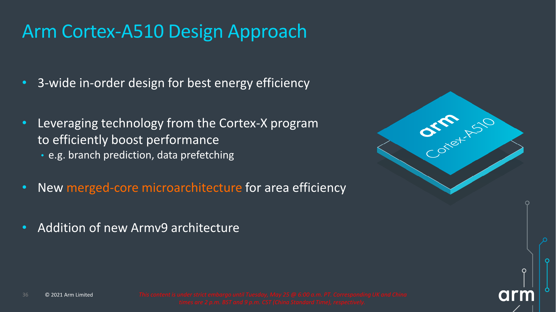
First of all, Arm made explicit note of the design’s continued use of an in-order execution flow, mentioning that in their view that this is still the most power-efficient way to design a core for such workloads. This remains a relatively controversial topic and point of discussion when put into context of Apple’s own out-of-order efficiency cores, a topic I’ll return on later.
Secondly, the Cortex-A510 introduces something called a “merged-core” microarchitecture, there’s some very high-level comparisons and similarities to what AMD had done with CMT in their Bulldozer cores a decade ago, but differs quite significantly in some important aspects in terms of the details and design.
Of course, like the X2 and A710, the A510 is an Armv9 design, and all three cores share the same architectural features with each other, allowing them to be integrated together into the same SoC. It’s to be noted that the A510, much like the X2, is a 64-bit only AArch64 core.
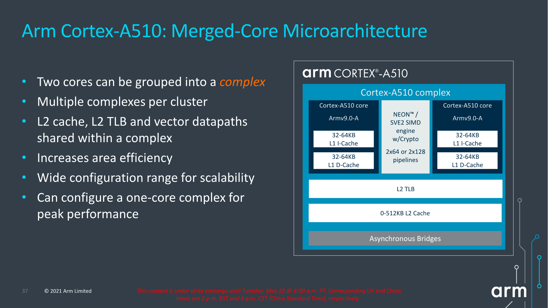
The most interesting aspect of the Cortex-A510 is the new merged-core approach. What Arm is doing here, is creating a new “complex” of up to two core pairs, which share the L2 cache system as well as the FP/NEON/SVE pipelines between them.
At first glance this will sound extremely similar to what AMD had done with Bulldozer and the CMT (Clustered Multithreading) approach, however Arm’s design is much more disaggregated in terms of what the actual cores are sharing. While AMD’s CMT module consisted essentially of a shared front-end between two integer back-ends and a single FP/SIMD back-end, Arm’s “merged cores” are actually full cores with their individual front-ends, mid-core, integer back-ends, and L1 cache hierarchies. The only thing being shared between the “cores” is the actual FP/SIMD back-end, as well as the L2 cache hierarchy.
Furthermore, while in the mobile market we expect vendors to use this new two merged cores per complex approach, it’s actually possible to simply just have a single core per complex. In which case the solo core would essentially have its own dedicated (non-shared) resources, but would be notably less area efficient than the intended merged core approach.
Generally, given the adoption of SVE2 and the relatively larger area footprint that the new execution backend requires, it makes sense to actually share these resources for these tiny new cores. Their typical workloads are also mostly only integer-bound background workloads which put less pressure on such units.
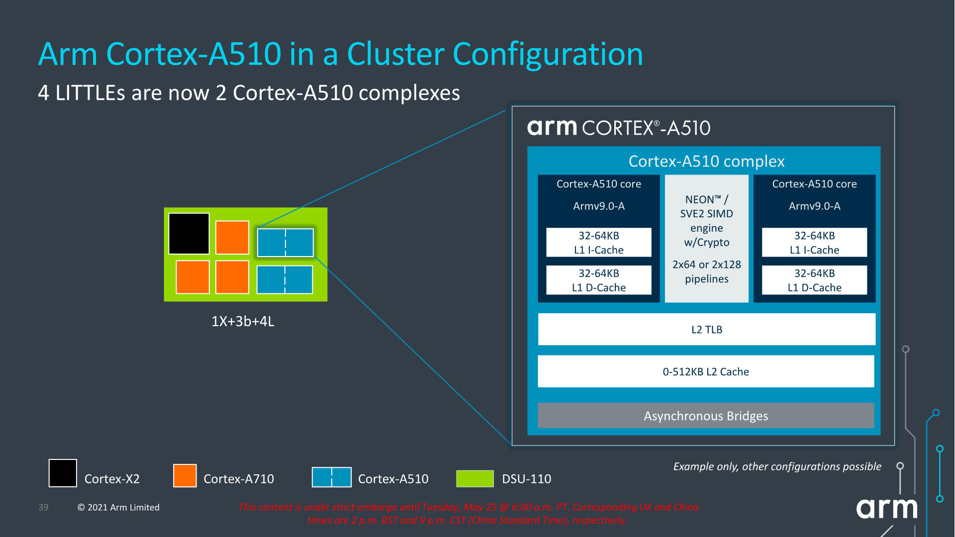
From a higher-level SoC standpoint, nothing really changes when it comes to the core-count, with the details being that we’ll be seeing two pairs or little cores now share a larger L2 cache between each other. This L2 can be configured up to 512KB, but as always, what we’ll actually see in products will very much depend on what vendors will want to implement into their designs. Because the new complex also only takes up a single interface on the DSU, it also opens up the possibility of designs larger than 8 “cores”, something I hope won’t happen, or hopefully only happens through more middle or big cores.
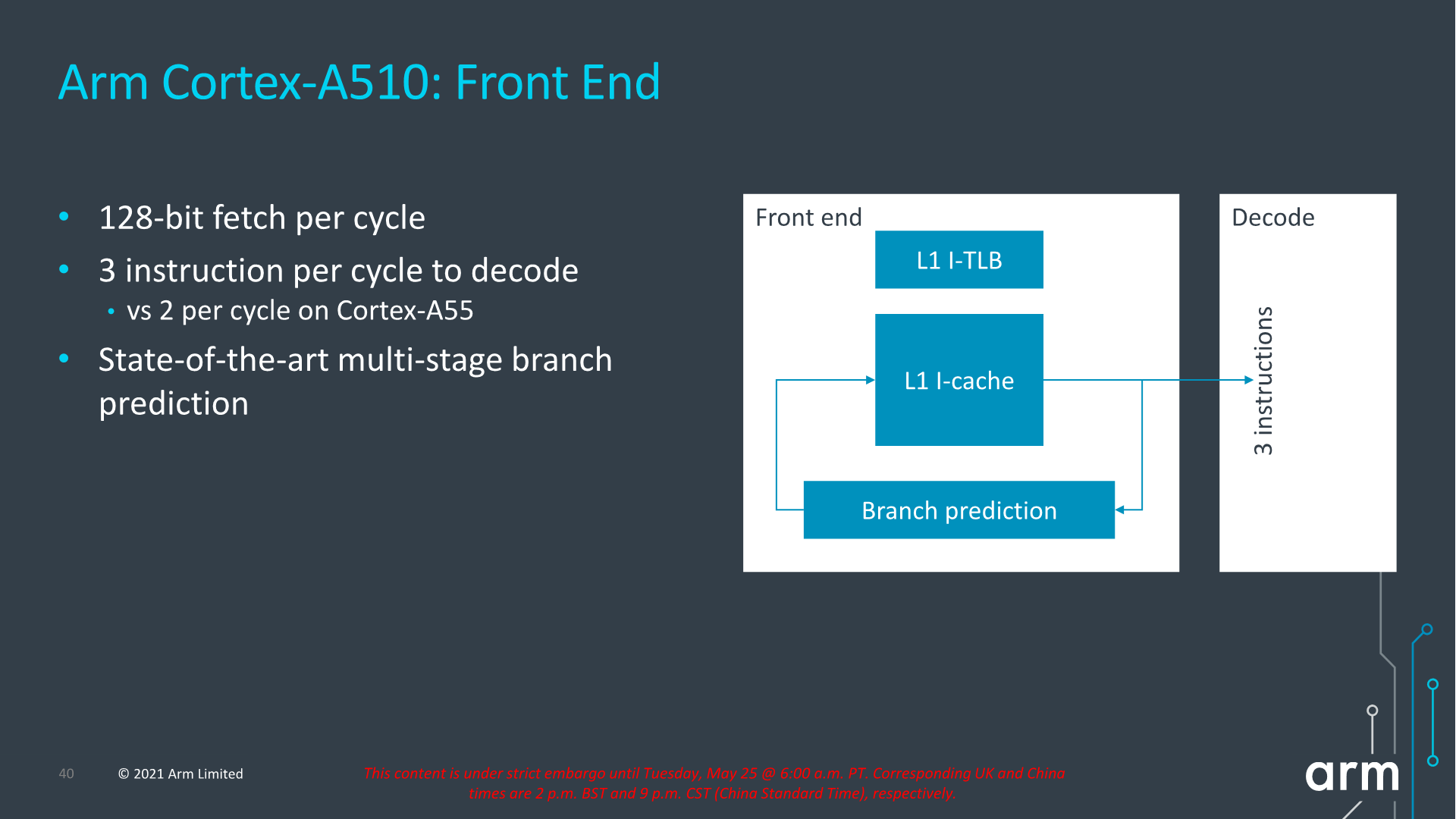
In terms of the front-end of the new A510, we’re seeing a 128-bit fetch pipeline which means it can fetch up to 4 instructions per cycle, giving the front-end a bit of leeway to close branch bubbles. The actual width of the decoder has increased from 2-wide to 3-wide.
In terms of branch prediction, as always Arm doesn’t disclose too many details, however the company did note that it used the same state-of-the-art approaches and techniques it uses on its larger cores. The L1 instruction cache can be either 32 or 64KB.

In terms of the shared vector execution back-end, it’s actually quite interesting here as Arm gives the option of either configuring the complex with smaller 2x64-bit pipelines or with 2x128b pipelines, the latter whose throughput would be 2x that of a Cortex-A55. I’m not too sure what mobile vendors will go with; we always hope for the larger configuration but as always, we’ll have to wait and see what will be employed in the actual products. In both configurations, the vector length is 128b as that’s the requirements for interoperability for the larger core microarchitectures.
Arm states that the shared pipelines are completely transparent to hardware, and that it’s also using fine-grained hardware scheduling. In actual multi-threaded workloads using both cores, the performance impact and deficit is said to only a few percent versus having a pipeline dedicated for each core. This is basically the cornerstone argument for why Arm has decided to use this more area-efficient merged-core approach.
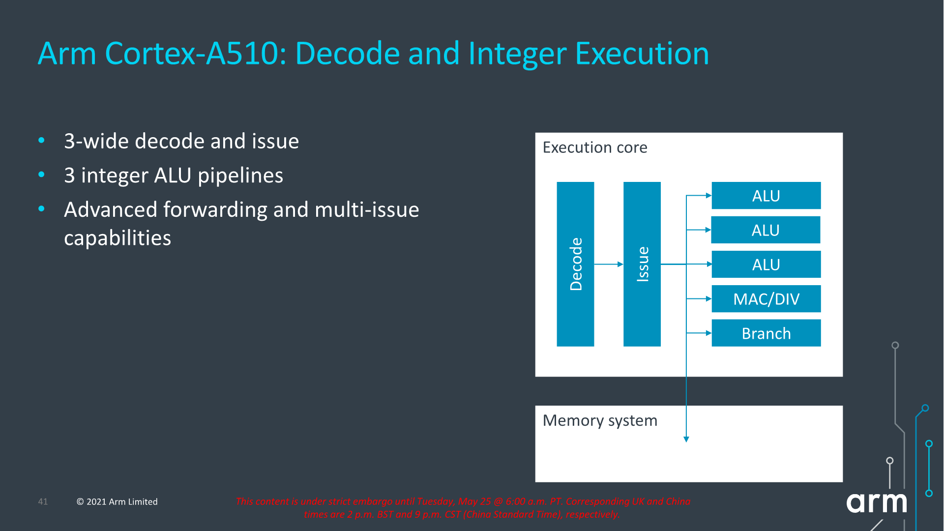
Although it’s an in-order architecture, Arm has still widened the back-end of the Cortex-A510 which now includes 3 ALUs, one complex MAC/DIV unit and a branch forwarding port. The explanation here is simply that there’s more opportunities to execute a wider variety of code blocks in fewer cycles when there’s a fitting sequence of instructions coming in to be executed.
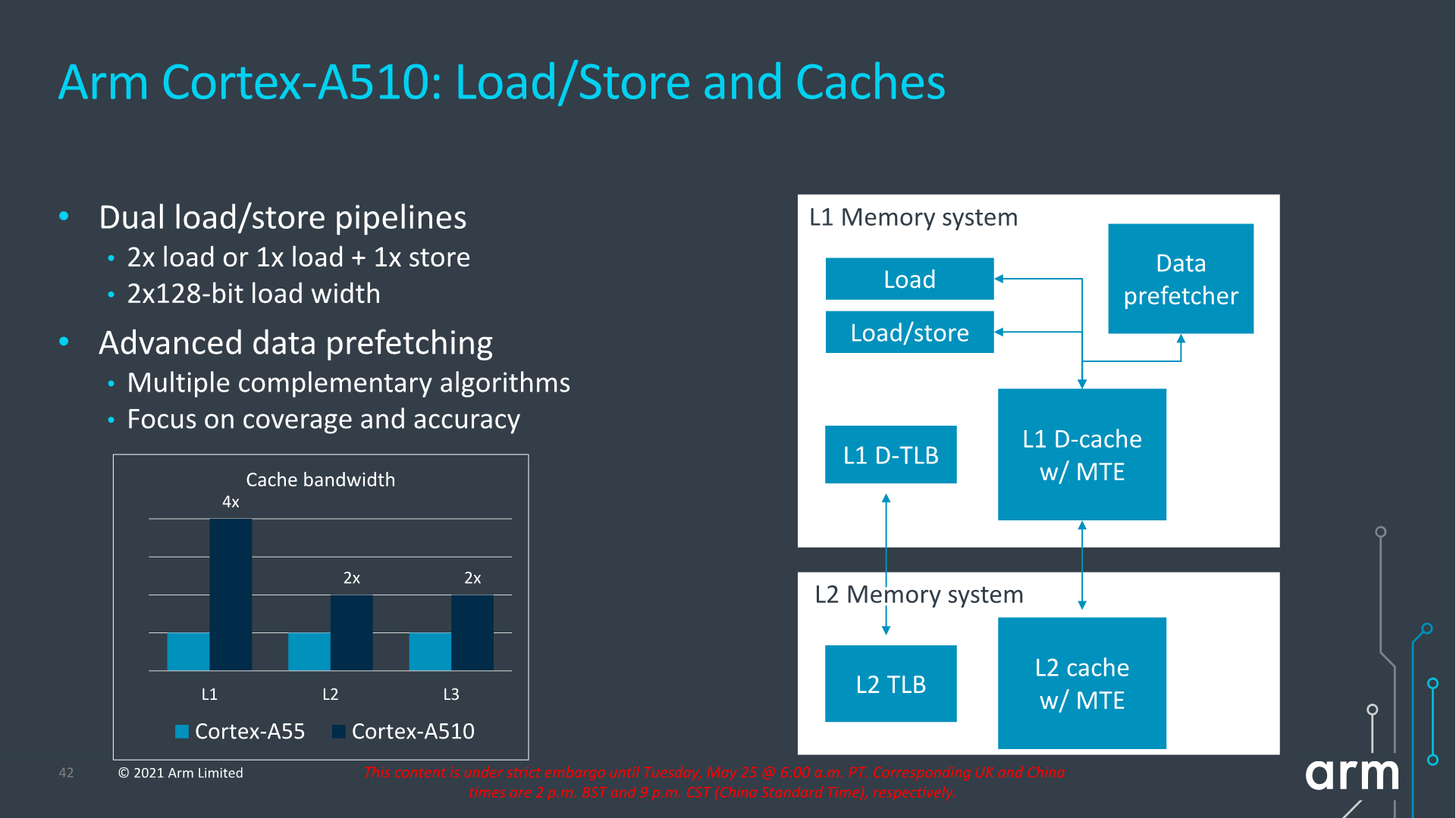
Finally, in the load-store system, the new structure is massively improved in comparison to the Cortex-A55 as we’re seeing a move from a load and store pipeline towards a load and a load/store pipeline, effectively doubling up on the number of loads executed per cycle. The width of the pipelines has also been increased with a doubling from 64b width to 128b width, so essentially load bandwidth compared to the Cortex-A55 is quadrupled.
The A510 also employs the similar very advanced prefetcher designs that we’ve seen in other recent big Arm cores, and adds to the large performance improvements that the core is able to achieve.
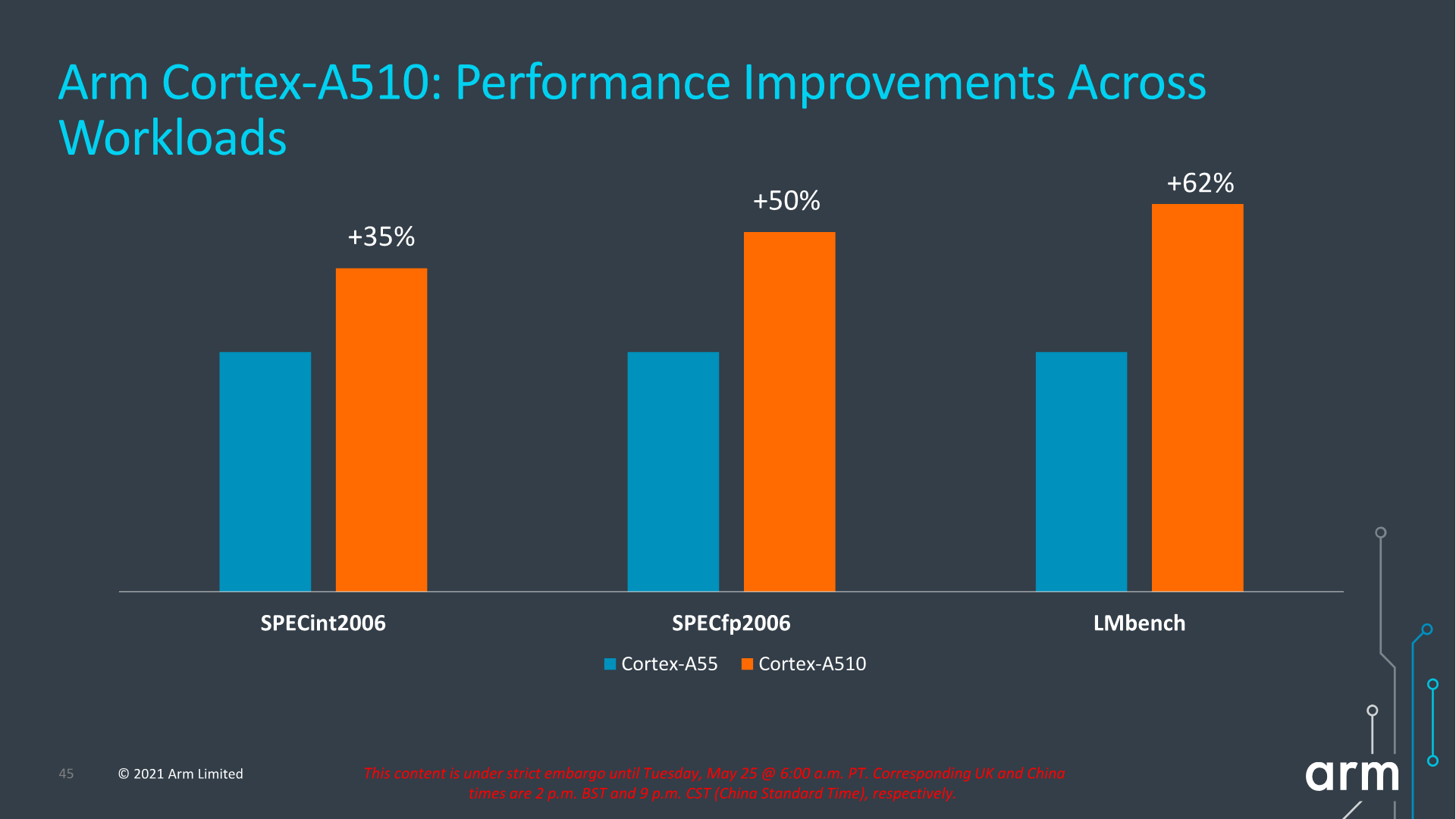
In terms of performance metrics, much like on the X2 and A710 presentation slides, the figures for the A510 aren’t very apples-to-apples as we’re comparing a Cortex-A55 with 32KB L1, 128KB L2 and 4MB L3 versus a Cortex-A510 with 32KB L1, 256KB L2 and 8MB L3. Frequency between the two cores is said to be the same. Under that scenario, we’re seeing +35% in SPECint2006 and +50% in SPECfp2006, which are seemingly very solid generational improvements, however given the cache hierarchy discrepancy as well as the fact that we’re comparing scores to a 4+ year old core, the actual improvements, especially from a compound annual growth rate (CAGR), doesn’t seem to be all that impressive.
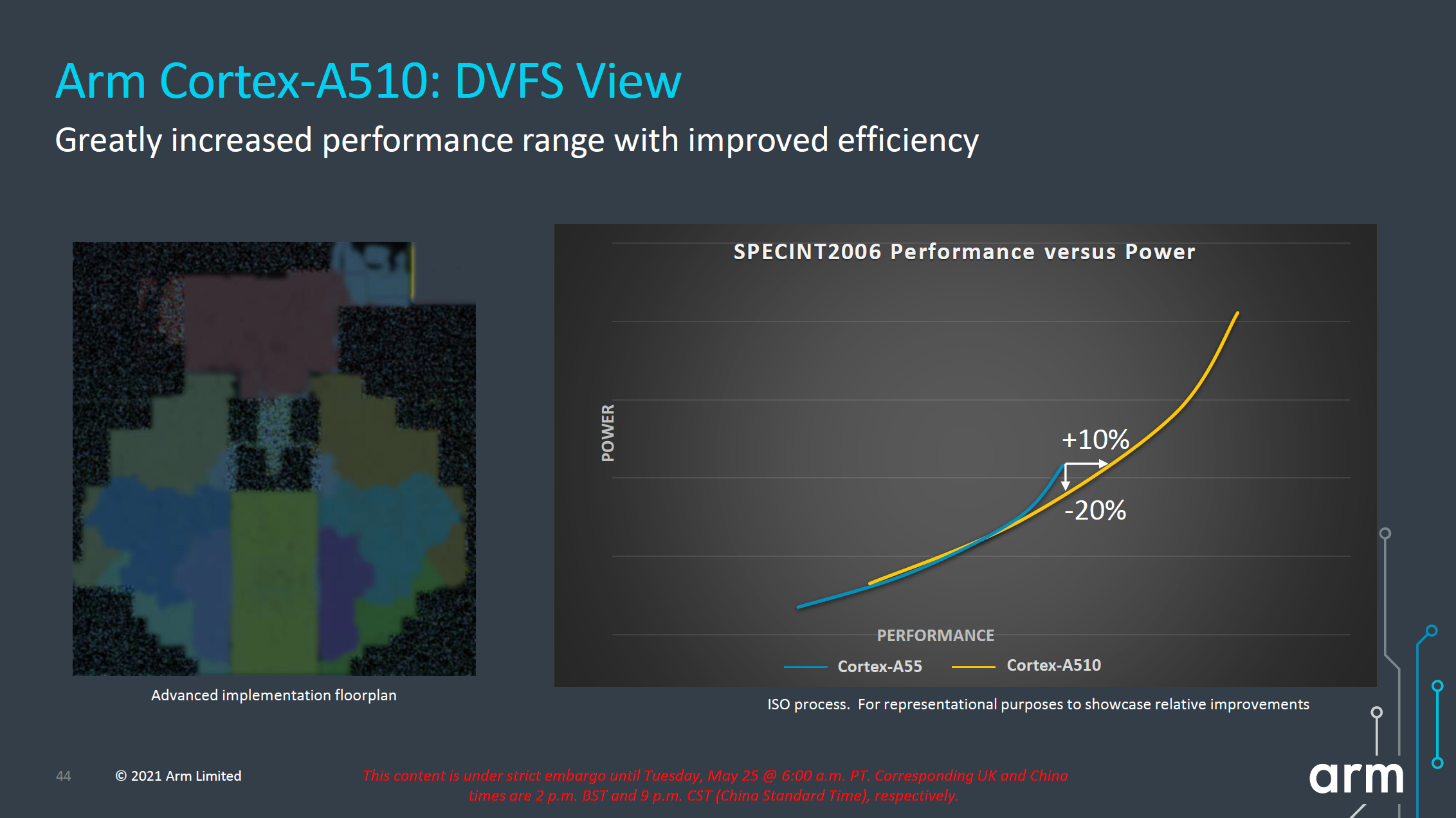
Looking at the projected performance and power curves on an ISO-process comparison, the new A510 seems rather lackluster from an efficiency standpoint. The ISO-power and ISO-performance gains are respectively +10% performance and -20% power, but the latter is really only valid for the high-end of the A55’s frequency curve, all the while the A510 pretty much overlaps the A55’s curve at lower operating points. While the A510 offers overall better performance, this seems to mostly be a product of extending the efficiency curve to higher power levels, and I was frankly disappointed to see this.
We’ll have to wait for the new generation SoCs to actually hit the market for us to test the new A510 cores, but if indeed they come with larger power consumption operating points to achieve higher performance, then Arm won't be much nearer in catching up to what Apple has been doing with their efficiency cores. As of the latest generation of SoCs, Apple’s efficiency cores were around 4x faster than any Cortex-A55 based SoC. Which, running at roughly the same system active power, also made them 3-4x more efficient in the traditional benchmarks. As presented, a theoretical A510 SoC won't be able to close that efficiency gap at all.
Arm is still adamant that for the kind of general use-cases in which the little cores are used in mobile phones – such as very light UI workloads – that their little core approach is still the most power-efficient way to achieve the best “DoU” or days of use figures. This is based in part on their internal projections as well as their partners', all of which indicate that the the triple issue in-order design they've developed is the most efficient option.
As the team explains it, it’s actually extremely hard to reproduce these more real-world workloads in any more structured benchmark (such as the typical test suites we tend to employ), but admitted there’s no real alternative that one could use to isolate performance and efficiency in such tasks. Generally, my counter-argument here is that iPhones still have outstanding battery life, so I’m still extremely skeptical on the whole lower-performance in-order core approach versus a more efficiency focused OOO core as demonstrated by Apple. Especially since we don’t really have an independent way to really test Arm’s claims, and the only data points we do have paint a very different picture.
Arm does note that this generation also had a lot of work done in regards to architectural features, and that the A510 is merely a starting point in a series of generations that are planned to be updated in a more regular fashion versus the large 4–5-year gap we’ve seen with the Cortex-A55 (just to be explicit, Arm doesn’t promise yearly updates, but we’ll be seeing successors in a much faster timeline). Those successors will see continued improvements in performance and power efficiency.
For this upcoming generation, the one benefit of the new little cores will come in more mixed-load workloads. Due to the DVFS nature of the various cores in an SoC, most core groups of a given core type share the same voltage rail and operate at the same frequencies. If there’s a primary thread workload that is resident on the middle cores at higher (less efficient) frequency operating points, any further medium-performance demand secondary threads that in the past couldn’t be serviced by A55 cores would have had to be migrated over to that much less efficient operating point on another middle core. On the A510 with its higher peak performance points, the workload would now be still be resident on the newer little cores, greatly increasing execution efficiency than if they were to be scheduled on the middle cores.
Overall, I’m still feeling a bit underwhelmed by the new A510 core, particularly given the 4 years it took to design it. Let’s hope that the upcoming mobile SoCs will have more apparent efficiency to them when we're testing them in 2022 devices.


181 Comments
View All Comments
ChrisGX - Thursday, May 27, 2021 - link
Using Andrei's initial performance estimate for the X1 (clocked at 3GHz) as a guide (47.2 SPECint2006) and ARM's own projection for the peak performance boost offered by the X2 over the X1 (+30% when process optimisations and frequency increases are factored in) we get a rating of 61.4 SPECint2006 for next years X series core. That is really a best case estimate and it is where the good news ends.The information we have on the 2022 Cortex cores does seem to lack the transparency of material of this sort that had been issued in earlier years by ARM. It is disappointing not to have any core frequency data in that information. A lot turns on realistic estimations of attainable core frequencies and having a good sense of power dissipation at maximum burst frequencies. We now know that Andrei's performance estimate for the X1 core wasn't borne out in practice (the actual performance exhibited by the highest performing X1 core - the one in the Snapdragon 888 - was 14% lower at 41.3 SPECint2006) owing to pitiful power dissipation characteristics of Samsung's 5nm LPE process that in order to prevent thermal build up and keep power consumption within budget on SoCs incorporating an X1 core SoC designers found it necessary to either a) reduce burst clock frequencies to below 3GHz or b) use restrictive power management controls to damp down chip operations threatening the thermal stability of the SoC that will naturally have the effect of throttling performance.
Using more realistic assumptions to project the likely performance of the X2 core (which I suspect might still be too optimistic because these forthcoming SoCs that incorporate an X2 core like the flagship Android smartphone SoCs of 2021 are said to be scheduled for production on Samsung fabs which must cast a degree of doubt on ARM's performance projections because recently Samsung's silicon process technologies have demonstrably failed to come up tp ARM's expectations) we get this number: 53.7 SPECint2006 (which represents the actual performance of the highest performing X1 core of 2021 x 1.3). Given the lack of transparency in the ARM data it is possible to entertain a rather broad range of imaginable SPEC peak integer performance ratings for the X2 core. A SPECspeed of 53.7 is my best guess.
ikjadoon - Tuesday, May 25, 2021 - link
These are geometric means of integer & FP scores. Typo for X1, ~50 not ~40. Let's be precise, now that I'm not on a phone ;)SPEC2006 1T Geomean:
A14 Firestorm = 71.72 points
A13 Lightning = 59.09 points
SD888 X1 = 49.48 points
Awarding the X2 the full 16% jump on both integer & FP, we can napkin math this to a Reference X2 = 57.40 at iso-frequency.
You're right they can (and maybe should) boost clocks so it could surpass the A13, but it's unrealistic to imagine Qualcomm shipping a 3.3+ GHz smartphone in 2022, especially if it's Samsung foundries again, but even on TSMC. Qualcomm's SD888 X1 at 2.84 GHz already ate 9621 joules (SPECint2006) and 4972 joules (SPECfp2006).
From https://www.anandtech.com/show/16463/snapdragon-88...
No one expects a literal doubling, but Arm's competition (NUVIA, Apple, Ampere) are not slowing down, either.
Wilco1 - Tuesday, May 25, 2021 - link
OK I get it now - the 40 made me think you meant SPECINT as that is what Cortex-X1 scored.3.3GHz on TSMC 5nm is conservative given it has significant performance/power improvements (which the A14 already benefits from), but yes it means switching back to TSMC.
Thala - Tuesday, May 25, 2021 - link
Indeed the performance gains of A14 vs. A13 are mostly frequency driven and much less IPC driven. It is not unreasonable to assume some frequency gains for X2 as well when moving to 5nm TSMC.Ppietra - Wednesday, May 26, 2021 - link
Thala, looking at the numbers IPC improved 8%, being responsible for 42% of performance growth... so not exactly much less!A13 to A14 transition gives no clue about what would happen between X1 and X2 or between Samsung and TSMC... X1 is already at 5nm, and its clock speed is just 5% less than the A14... Their designs priorities are also different, so you cannot infer much!
name99 - Tuesday, May 25, 2021 - link
All true. But of course A14 is an especially easy opponent!- it's the last round of what appears to be Apple's 4-year "seriously new micro-architecture" cadence -- A77..A10 as gen 1, A11..A14 as gen 2, A15 et seq as gen 3.
- it was clearly designed with the single highest priority being get the x86 stuff working. Meaning that anything that did not match that priority (including, eg, optimized physical layout and risky micro-architectural innovations) was punted till the A15
- it doesn't have SVE/2, which is good for anything up to a 80% speed boost depending on the exact code (even with just compiler vectorization). Averaging over "representative code bases" is a game that's never going to get everyone to agree, but the one attempt I saw to do this came up with an average performance boost of ~30%.
Given how *low* ARM's numbers are, I assume they're talking about performance in the absence of use of SVE/2? Honestly the whole thing is kinda weird, how little they're pushing the SVE/2 angle and how much one might expect it to improve things.
I do *not* expect Apple to be as timid... And while Apple tend to shy away from hardware announcements at WWDC, we all know about M1 by now, AND we know that SVE/2 will be in next year's ARM (so presumably in this year's Apple). Meaning maybe there will be some talks about SVE/2 (and other ARMv9 stuff) at WWDC?
Wilco1 - Tuesday, May 25, 2021 - link
You are exaggerating the gains of SIMD in general. Yes automatic vectorization helps, but even if it improves some image transformations by 80%, it's never going to speed up browsing by 30%. Or any other general purpose code. Or SPEC.Remember this is 128-bit SVE, so 4 Neon units are about as fast as 4 SVE units. For great SVE performance on HPC code look at A64FX or the upcoming Neoverse V1.
name99 - Tuesday, May 25, 2021 - link
- One hopes that the combination of agnostic length and predicates will allow a lot of code for which vectorization was previously uneconomical (too expensive to mask out fiddly bits, too much overhead in loop prologs and epilogs) to now be handled. We shall see.- You are right about the 128b of course; yet another instance of ARM never trying for a stretch goal! I assume Apple will be implementing this as 2x256, meaning, among other things, the path from L1D to LSU grows from 128b to 256b wide, and that's an example of where SVE/2 (indirectly, sure) helps boost performance for everyone.
smalM - Friday, May 28, 2021 - link
Could you please explain why you asume Apple will reduce the number of FP/SIMD units in exchange for widening them. Is that really better? From a FP or from a SIMD standpoint?Thanks in advance.
Making the path from L1D to LSU 256b wide is something Apple could do anyways and is not directly related to SVE2; I was astonished they didn't do it when they added the fourth FP/NEON unit.
mode_13h - Saturday, May 29, 2021 - link
> would you please explain why you asume Apple will reduce the number of FP/SIMD units> in exchange for widening them. Is that really better?
For SVE it's a little better, since it means software having to run loops for about half as many iterations, correspondingly reducing loop overhead.
> Making the path from L1D to LSU 256b wide is something Apple could
> do anyways and is not directly related to SVE2
I don't really see why. It seems like it'd only help for back-to-back reads or writes from/to consecutive addresses. And if 128-bits is already enough to do that, then extra width would be a waste.