Arm Announces Neoverse V1, N2 Platforms & CPUs, CMN-700 Mesh: More Performance, More Cores, More Flexibility
by Andrei Frumusanu on April 27, 2021 9:00 AM EST- Posted in
- CPUs
- Arm
- Servers
- Infrastructure
- Neoverse N1
- Neoverse V1
- Neoverse N2
- CMN-700
First Thoughts & End Remarks
2020 was indeed a super-exciting year for Arm’s server ambitions, and one can easily claims that then Neoverse N1 has been a resounding success and implementations can be seen as being on the same playing field as the best that AMD and Intel are able to achieve, even against today’s newest generations.
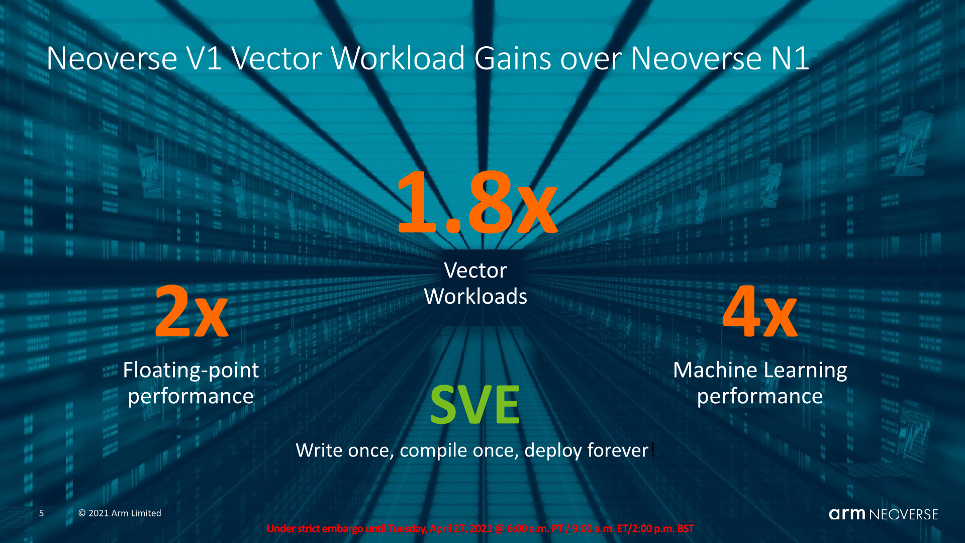
The new Neoverse V1 and N2 continue the story in a 2-prong approach. For the Neoverse V1, back when the design was initially teased back in September, I was quite amazed at the claim of +50% IPC. After today’s figures, while the design is still very impressive, the disclosures of the power, area, and resulting power efficiency requirements have somewhat dulled my expectation of the new CPU microarchitecture.

What’s clear about the Neoverse V1 is that this seems to really be an HPC-oriented design. Alongside the known SiPearl Rhea chip, backed by the European Processor Initiative’s goals for HPC uses, Korea’s ETRI (Electronics and Telecommunications Research Institute) also has a V1 designed dubbed “K-AB21” in the works, also with hybrid HBM2E and DDR5 memory. Along with today’s announcement of the V1, India’s Center for Development of Advanced Computing has also announced that they’re a V1 licensee and be using it in an exascale supercomputer project.
Essentially, it seems the V1 will serve as the foundation of many new custom HPC projects, which is a great win both for Arm as an IP vendor, as well as their licensees which are able to build something to their exact needs.
For enterprise and cloud usages, given the CPU’s power efficiency, I now doubt that we’ll somehow see implementations from cloud or merchant silicon vendors such as Amazon or Ampere, particularly because the N2 will be available.
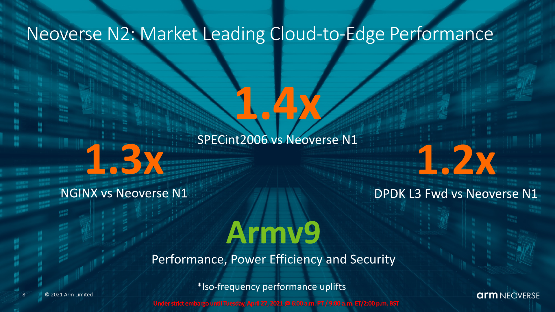
The Neoverse N2 is a more straightforward migration from the N1. IPC is improved by significant amounts which should result in good generational performance increases. I have concerns about power efficiency as the performance increases come at a linear cost of increased power. There’s a one-time opportunity to increase performance in many workloads by closing the power-gap for workloads which do not fully fill the TDP of a system today (while throttling others), however any further performance increases beyond that are dependent on actual good physical implementations by the vendors to fully take advantage of the next-generation process nodes and to execute on those theoretical gains. We’ll see how that will pan out – for now I’ll give the Arm the benefit of doubt, however we’ll also see similar gains in 5nm designs from the likes of AMD. How the competitive situation will end up in 2022 remains to be seen.
Arm had also made a note that while the N2 is a newer generation IP than the V1, roughly a year apart in design, the company actually expects for N2 products to come out only shortly after V1 products, sometime by end of this year. This further enforces my view that we’ll probably not see much V1 designs outside of the HPC market, and that Amazon and Ampere are likely to follow up with N2 based Gravitons and Altras. I want to be explicit here that none of the usual cloud vendors / CSPs / hyperscalers have yet officially commented on what kind of IP they'll be using in the next-generation designs.
The star of the show today was I think the CMN-700, and the vast new flexibility it allows vendors to achieve. The new architectural improvements and the move towards CCIX 2.0 and CXL are definitive big advances that will allow licensees to create more exotic designs. At the very least, it allows for effective usage of chiplet architecture designs, which is a much-needed feature that vendors need to adopt to be able to ensure affordability and manufacturability of products on leading edge nodes.
I’ll be looking forward to new V1 and N2 designs in 2022, and hope we’ll hear more details from licensees through the course of the year.


95 Comments
View All Comments
name99 - Thursday, April 29, 2021 - link
What do you mean by "compare?"Apple is 8-wide Decode, Map, Rename. But that doesn't include the fact that Apple does a ton of clever work in those three stages (
- simple branches handled at Decode,
- a variety of zero-cycle moves and immediate handling in Rename
- two-level scheduler, with the higher level able to accept an 8-wide feed from Rename, even though the lower-level scheduler is narrower [6 for int, 4 for FP or LS] )
Apple is *astonishingly* wide at the completion end. 16-wide register freeing and history file release, up to 56(!!!)-wide release of ROB entries.
The Apple pattern so far (insofar as pattern-detection is worth anything) has been a 1st generation of four cores (A7/8/9/10) with similar design and 6-wide, constantly iterating on details within that framework;
then a 2nd generation (A11/12/13/14) that makes explicit the big.LITTLE structure (in A10 that was mostly invisible) and based on an 8-wide (with 6 integer units) structure.
If one has to bet, the reasonable thing to bet might be something like starting with A15 we transition to 10-wide (initially with6 later with 8 integer units), and 2xSVE256. Once again lay the framework, then scale out the pieces over the subsequent three cores.
One thing that is very clear (and presumably part of Apple's success) is that they have been very willing to keep modifying how they do things; they don't just settle on a design and leave it unchanged except perhaps for some scaling up. For example the way they handle the MOV xn, xm instruction has gone through at least three very different schemes. This may seem trivial (who cares about how a singe instruction is implemented?) except that these schemes indicate a substantial reworking of the entire register file and how registers are allocated and then freed.
This is in comparison to x86 which seems to live in (probably justified) terror that any change they make, no matter how low level, will probably break something because the whole system is so complex and so interconnected that no one person holds the entire thing in their head.
They also seem to have a good system in place for hiding new functionality behind chicken bits, so that they can effectively debug new features within shipping hardware. For example there are reasons to believe that A14 might have in place most of the pieces required for physical register file amplification (avoid allocation for back-to-back register usage and grab the intermediary off the bypass bus; early release of logically overwritten registers) but these are not visible -- probably behind chicken bits so that they can be tested under all circumstances in shipping HW, and made visible for A15.
And anyone who has not looked at the details is unaware of just how impressive the underlying Apple µArch platform is. There is substantial room there on-going growth! As I continue to explore it, not only do I see how well it works today, I also see multiple directions in which it could "easily" (ie feasibly, on schedule and within budget) be improved for years to come. The only other artifact I know of that comes close in terms of quality of implementation and ability for continuing growth is the Mathematica code base -- other artifacts like other CPUs, or various OS implementations, are in a totally different (and far inferior) league.
name99 - Thursday, April 29, 2021 - link
To expand on my point, it's great that ARM are including so many good idea, but it's also astonishing the extent to which pretty much every good idea already has an Apple precedent.For example consider the MPAM discussion: "The mechanism to which this can be achieved can also include microarchitectural features such as dispatch throttling where the core slows down the dispatched instructions, smoothing out high power requirements in workloads having high execution periods, particularly important now with the new wider 2x256b SVE pipelines for example."
This sounds like (and IS) a good idea -- certainly a lot better than reducing frequency the way Intel does for AVX512.
But look at this Apple patent from 2011(!)
https://patents.google.com/patent/US9009451B2
"A system and method for reducing power consumption through issue throttling of selected problematic instructions. A power throttle unit within a processor maintains instruction issue counts for associated instruction types. The instruction types may be a subset of supported instruction types executed by an execution core within the processor. The instruction types may be chosen based on high power consumption estimates for processing instructions of these types. The power throttle unit may determine a given instruction issue count exceeds a given threshold. In response, the power throttle unit may select given instruction types to limit a respective issue rate. The power throttle unit may choose an issue rate for each one of the selected given instruction types and limit an associated issue rate to a chosen issue rate. The selection of given instruction types and associated issue rate limits is programmable."
I just keep bumping into this stuff! Arm release new cores with what seem like good ideas (and of course ARM tell us a lot more about what's new than Apple does). I do some exploring -- and find Apple patented that idea five or more years earlier!
mode_13h - Thursday, April 29, 2021 - link
> consider the MPAM discussionThe slide calls that MPMM. The article confuses it with Memory Partitioning And Monitoring.
Anyway, the N2's PDP sounds a lot more advanced.
GeoffreyA - Friday, April 30, 2021 - link
Zen 3 needn't blush when standing next to Apple. 4-wide decode might be small but that does pick up to 6, coming out of the micro-op dispatch. Then, going down, you've got 10-wide issue on the INT side, and 6-wide on FP. Admittedly, narrower register files and 8-wide retire from the (smaller) ROB, along with smaller caches. As for move elimination, even Skylake has that. Yes, everything tends to be narrower. But I think it goes to show there's nothing particularly out of this world on the Apple side.name99 - Friday, April 30, 2021 - link
I did not say that move elimination was the interesting part.I said that what was interesting is that over Apple's short CPU career they have already implemented it in three significantly different ways.
That strikes me as interesting and important -- there is no resting on the laurels, no acceptance that "we have the feature, OK to slow down". You honestly believe that Intel operates according to that same mentality?
GeoffreyA - Friday, April 30, 2021 - link
I'll admit, Apple isn't resting; and they aren't scared to break orthodoxy in advancing their designs. If the others do not wake up, they'll be left in the dust. As for Intel, complacency has put them in the well-deserved pickle they're in today. AMD deserves credit, though, for doing much these past few years; and, like Apple, aren't resting on their laurels either (arguably like they did in the K8 era).mode_13h - Friday, April 30, 2021 - link
How big are Apple's cores, though? Area is tricky, because they tend to be on a newer process node.But, my point is that maybe AMD and Intel aren't making their cores even larger and more complex, because they're targeting the server market and found that a more area-efficient way to scale performance is by adding more cores, rather than making their existing cores even more complex.
name99 - Friday, April 30, 2021 - link
A14 is 88mm^2.Eyeballing it, each large core is about 2.5% of that area, so 2.2mm^2
Throw in the L2 at about 3.5%, so 3mm^2 (shared between two cores).
Throw in the SLC (not exactly an L3, but pretend it is if you insist) at 8.8% and about 8mm^2.
I guess if you were targeting a server type design, we could probably treat it as something like
2.5+(3/4)+ (8.8/8) [making rough guesses about what sort of L2 and L3 would be optimal for a server type design] so ~4.4mm^2.
Could fit ~100 in a 440mm^2 (though you'd also want some memory controllers and IO!)
Definitely a lot larger than something like an N1 or N2 -- but of course, Apple isn't designing for the data center -- if they were, they'd probably adopt something halfway between Fire Storm and Ice Storm.
The problem is not that Intel and AMD are chasing the server market, it is that the way they are chasing it is incoherent. IF your primary goal is the server market, then WTF are you designing for super-high frequencies? The data center cores never run at those frequencies -- but being able to boast about them means your transistor density is half to a third that of Apple (or more relevant ARM/Altra/Graviton) on the same process...
Pick a goal and optimize for it! But Intel's goal seems to be to optimize for marketing that they can hit 5.x GHz (for half a second...) Not clear that designing the entire company around that goal (of zero interest to the data center, and little interest to most users) is such a great long-term strategy.
mode_13h - Saturday, May 1, 2021 - link
> IF your primary goal is the server market, then WTF are you designing for super-high frequencies?AMD actually has lagged Intel in frequency, and I think that's one of the reasons. Remember, AMD is the only one using the same exact silicon on both the mainstream desktop and in all their server products.
Intel, on the other hand, has completely separate silicon for their server dies, and we don't know all of the subtle ways they could differ from their desktop or laptop cores. We just know they tend to reuse the same basic core micro-architecture up and down their product lines (except for the really cheap/low-power stuff).
> The data center cores never run at those frequencies
A few Cascade Lake Xeons could turbo up to 4.5 GHz, which benefits certain workloads. The fastest turbo clock of an Ice Lake Xeon is 4.4 GHz
The fastest EPYC can boost up to 4.1 GHz.
In Intel & AMD's defense, a simpler core can clock higher, but runs more efficiently at lower clocks and enables higher densities. So, it seems like a pretty good strategy to me.
> Pick a goal and optimize for it!
Like ARM, Intel and AMD trying to balance power (in a server/laptop application, at least) and area. Apple is the only one who really has the luxury not to care much about area and just optimize for a single target. When Apple reuses its laptop core micro-architecture in both desktops AND servers, then we can compare them to the other guys. Until then, I think it's a case of Apples and pears.
GeoffreyA - Saturday, May 1, 2021 - link
"Until then, I think it's a case of Apples and pears."I think that's it. Well, soon process improvements will be a thing of the past, owing to quantum effects, and then we'll see who does what. The free ride is almost over.