Arm Announces Neoverse V1, N2 Platforms & CPUs, CMN-700 Mesh: More Performance, More Cores, More Flexibility
by Andrei Frumusanu on April 27, 2021 9:00 AM EST- Posted in
- CPUs
- Arm
- Servers
- Infrastructure
- Neoverse N1
- Neoverse V1
- Neoverse N2
- CMN-700
The Neoverse V1 Microarchitecture: X1 with SVE?
Starting off with the new Neoverse V1, the design is both of a familiar origin, but also has a few distinct features that we see for the first time ever in an Arm CPU. As noted in the introduction, the V1 was designed at the same time as the Cortex-X1 by the same team at Arm’s Austin design centre, with large similarities between the two microarchitectures when it comes to the block structures.
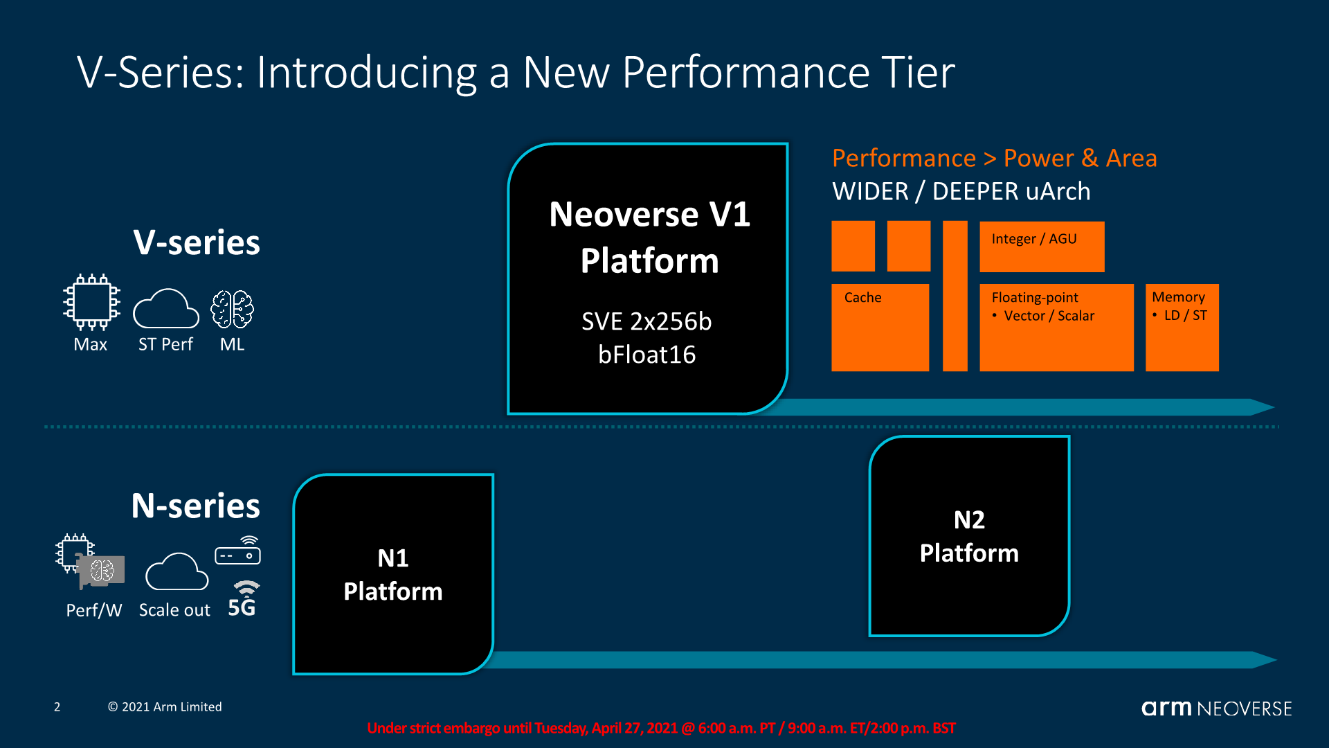
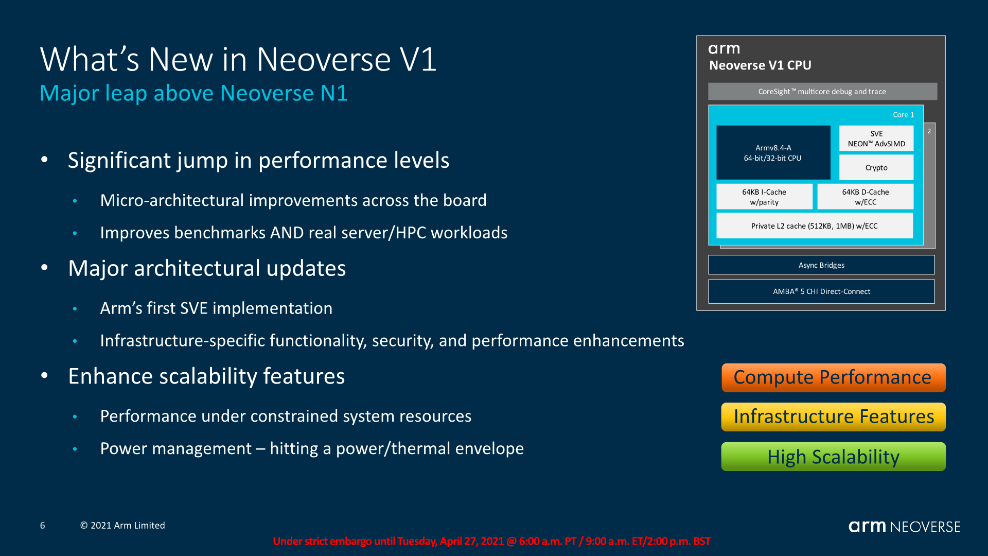
What’s notable about the V1, in comparison to the X1 and of course the predecessor N1, is the fact that this is now an SVE capable processor, with two native 256b SIMD pipelines, and also introducing server-only features such as coherent L1I caches, bFloat16 execution capabilities, and a slew of distinct characteristics we’ll cover in just a bit.
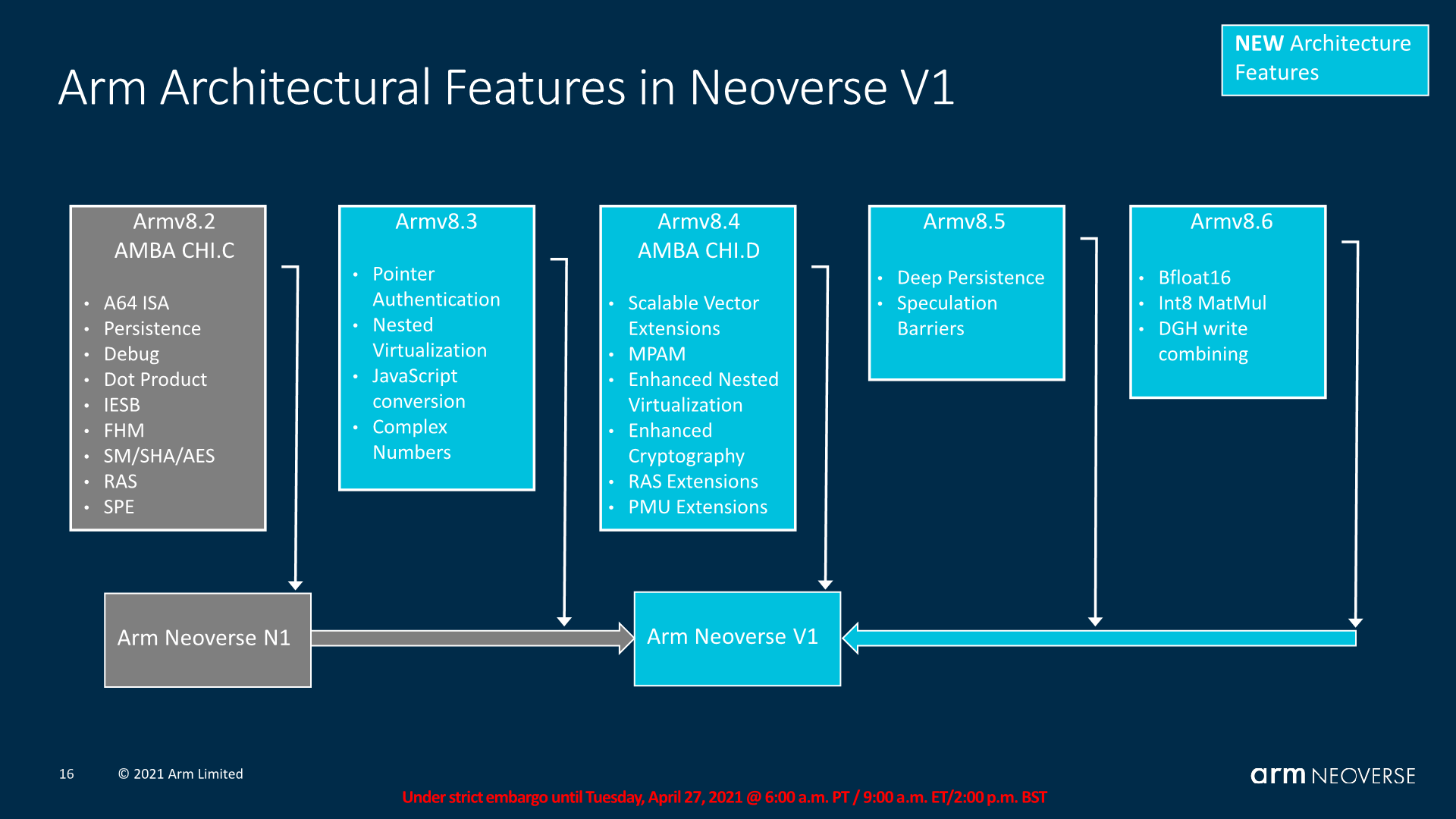
The architectural features of the Neoverse V1 are probably the most complicated in terms of describing – essentially, it’s a v8.4 baseline architecture which also pulls v8.5 and v8.6 features in for the HPC oriented workloads the design is aimed for. Given that we talked about Armv9 only a month ago, this may seem a bit odd, but again we have to remember that the V1 has been designed some time ago and that customers have had the IP for quite a while now, taping in or having already taped out V1 processors.
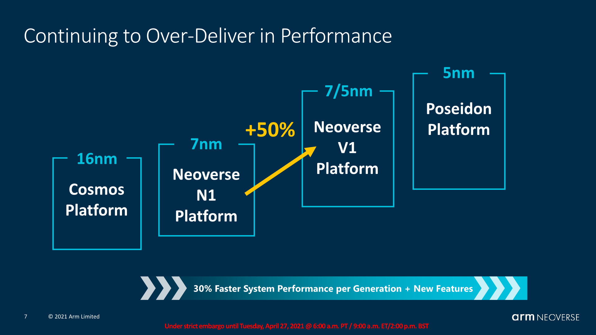
The big promise of the V1 is its extremely large performance jump over the N1, coming in at an IPC increase of +50%. This sounds large, and it is, but it’s also not all that surprising given that the microarchitecture essentially is 2 microarchitecture design generations newer than the N1, even through from a infrastructure product standpoint it’s only one generation newer.

From a high-level pipeline standpoint and microarchitecture view, the Neoverse V1 is very similar to the X1. It’s still an extremely short pipeline design that has a minimum of 11 stages, with Arm putting a lot of focus on this aspect of their microarchitectures to reduce branch misprediction penalties as much as possible. This aspect of the microarchitecture has remained relatively static over the last few iterations of the Austin family of designs starting with the A76, so Arm notes that the frequency capabilities of the V1 is essentially unchanged when compared to the N1, with performance boosts coming solely from increased IPC.

The V1 sees a lot of the front-end improvements we’ve seen with the Cortex-A77 and Cortex-X1 generations, which saw larger front-end branch improvements such as a doubled up bandwidth for the decoupled fetch unit, much larger L2 BTB to up to 8K entries, and a rearranging and resizing of the lower level BTBs, with the L0 (nanoBTB) growing to 96 entries, and the L1 BTB (microBTB) no longer being present when compared to the Neoverse N1.
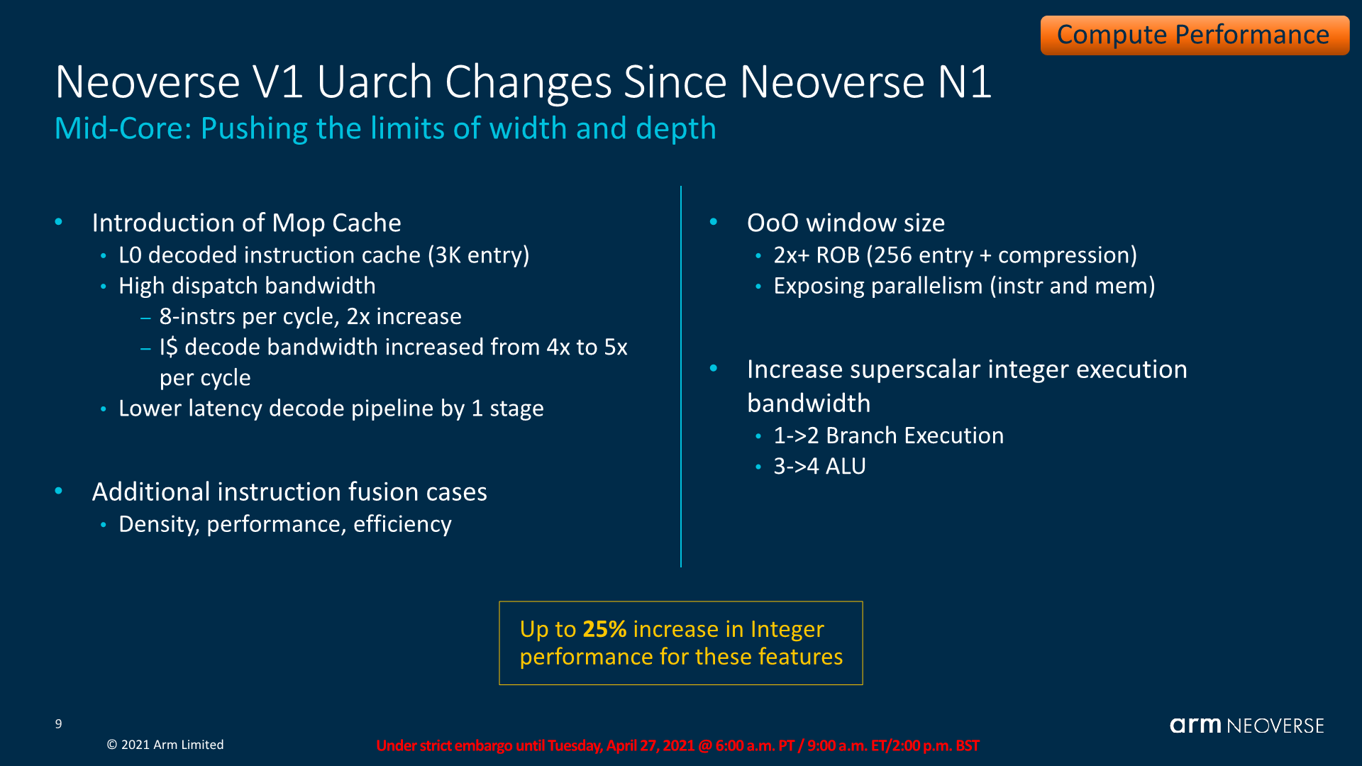
The V1 one when compared to the N1 also adds in new structures that hadn’t been present in the design, such as the introduction of a macro-Op cache of up to 3K decoded instructions. The dispatch bandwidth from the Mop cache is 8-wide, while the actual instruction decoder this generation is 5-wide, much the same as on the X1.
The out-of-order windows size is essentially doubled when compared to the Neoverse N1, with the ROB growing to 256 entries. This is actually a tad larger than what Arm was willing to disclose for the Cortex-X1 where the company had only talked about a “OoO window size of 224”, so in this regard this seems to be a differentiation to what we’ve seen in the X1.
On the back-end integer execution pipelines, the design also pulls in the many changes we’ve seen with the A77 generations, which amongst others include a doubling of the branch execution ports, and a new complex ALU capable of simple instructions such as additions as well as more complex operations such as multiplications and divisions.
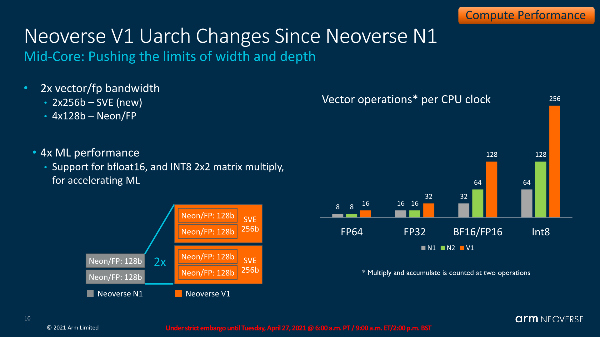
Obviously enough, the new SIMD pipelines are very different on the V1 given that this is Arm’s first ever SVE capable microarchitecture. The design has two pipelines with seemingly two dedicated schedulers, with native capability for 256b wide SVE vectors. The design is fully backwards compatible for 128b NEON/FP operations in which the pipelines then essentially act as 4x128b units, meaning it has the same execution width as the X1 in that regard.
Compared to the N1, the new design also supports new bFloat16 and Int8 data formats which greatly increase the AI and ML inferencing performance capabilities of the core.
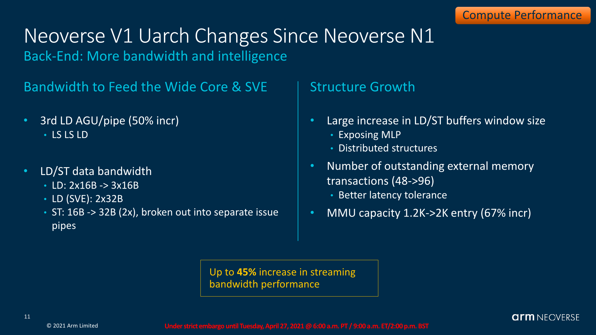
On the memory subsystem side, we also see the increased unit count found on the Cortex-X1, including 2 load/store units and one load unit, meaning the core is capable of up to 3 loads per cycle and 2 stores per cycle maximum. SVE vector bandwidth is 2x32B per cycle for loads, and 32B per cycle for stores.
The core naturally includes the data parallelism improvements seen on the X1 in order to increase MLP (Memory-level parallelism) capabilities.
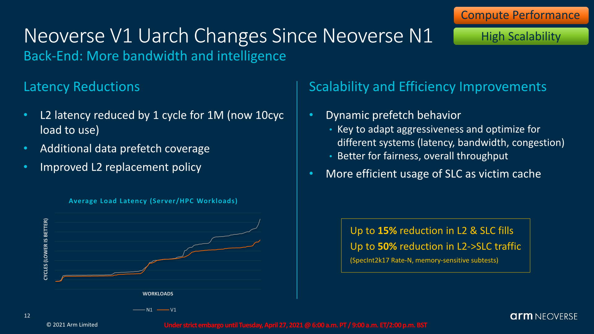
The L2 cache has also adopted a similar design to that of the X1, which is now 1 cycle faster at the same 1MB size, and has double the number of banks in order for increased access parallelism.
Arm here discloses a quite large reduction in the system level latency for the V1. Besides structural improvements, new generation prefetchers are a big part of this, such as the introduction of a new type of temporal prefetcher which is able to latch onto arbitrary access patterns over time and recognise subsequent iterations of the same pattern, and pull the data in.
Arm discloses that the core has new dynamic prefetching behaviour that plays a major role in reducing L2 to interconnect traffic, which is a critical metric in large core count systems where every byte of bandwidth needs to be of actual use and cannot be wasted for wrongly speculated prefetching.


95 Comments
View All Comments
name99 - Thursday, April 29, 2021 - link
What do you mean by "compare?"Apple is 8-wide Decode, Map, Rename. But that doesn't include the fact that Apple does a ton of clever work in those three stages (
- simple branches handled at Decode,
- a variety of zero-cycle moves and immediate handling in Rename
- two-level scheduler, with the higher level able to accept an 8-wide feed from Rename, even though the lower-level scheduler is narrower [6 for int, 4 for FP or LS] )
Apple is *astonishingly* wide at the completion end. 16-wide register freeing and history file release, up to 56(!!!)-wide release of ROB entries.
The Apple pattern so far (insofar as pattern-detection is worth anything) has been a 1st generation of four cores (A7/8/9/10) with similar design and 6-wide, constantly iterating on details within that framework;
then a 2nd generation (A11/12/13/14) that makes explicit the big.LITTLE structure (in A10 that was mostly invisible) and based on an 8-wide (with 6 integer units) structure.
If one has to bet, the reasonable thing to bet might be something like starting with A15 we transition to 10-wide (initially with6 later with 8 integer units), and 2xSVE256. Once again lay the framework, then scale out the pieces over the subsequent three cores.
One thing that is very clear (and presumably part of Apple's success) is that they have been very willing to keep modifying how they do things; they don't just settle on a design and leave it unchanged except perhaps for some scaling up. For example the way they handle the MOV xn, xm instruction has gone through at least three very different schemes. This may seem trivial (who cares about how a singe instruction is implemented?) except that these schemes indicate a substantial reworking of the entire register file and how registers are allocated and then freed.
This is in comparison to x86 which seems to live in (probably justified) terror that any change they make, no matter how low level, will probably break something because the whole system is so complex and so interconnected that no one person holds the entire thing in their head.
They also seem to have a good system in place for hiding new functionality behind chicken bits, so that they can effectively debug new features within shipping hardware. For example there are reasons to believe that A14 might have in place most of the pieces required for physical register file amplification (avoid allocation for back-to-back register usage and grab the intermediary off the bypass bus; early release of logically overwritten registers) but these are not visible -- probably behind chicken bits so that they can be tested under all circumstances in shipping HW, and made visible for A15.
And anyone who has not looked at the details is unaware of just how impressive the underlying Apple µArch platform is. There is substantial room there on-going growth! As I continue to explore it, not only do I see how well it works today, I also see multiple directions in which it could "easily" (ie feasibly, on schedule and within budget) be improved for years to come. The only other artifact I know of that comes close in terms of quality of implementation and ability for continuing growth is the Mathematica code base -- other artifacts like other CPUs, or various OS implementations, are in a totally different (and far inferior) league.
name99 - Thursday, April 29, 2021 - link
To expand on my point, it's great that ARM are including so many good idea, but it's also astonishing the extent to which pretty much every good idea already has an Apple precedent.For example consider the MPAM discussion: "The mechanism to which this can be achieved can also include microarchitectural features such as dispatch throttling where the core slows down the dispatched instructions, smoothing out high power requirements in workloads having high execution periods, particularly important now with the new wider 2x256b SVE pipelines for example."
This sounds like (and IS) a good idea -- certainly a lot better than reducing frequency the way Intel does for AVX512.
But look at this Apple patent from 2011(!)
https://patents.google.com/patent/US9009451B2
"A system and method for reducing power consumption through issue throttling of selected problematic instructions. A power throttle unit within a processor maintains instruction issue counts for associated instruction types. The instruction types may be a subset of supported instruction types executed by an execution core within the processor. The instruction types may be chosen based on high power consumption estimates for processing instructions of these types. The power throttle unit may determine a given instruction issue count exceeds a given threshold. In response, the power throttle unit may select given instruction types to limit a respective issue rate. The power throttle unit may choose an issue rate for each one of the selected given instruction types and limit an associated issue rate to a chosen issue rate. The selection of given instruction types and associated issue rate limits is programmable."
I just keep bumping into this stuff! Arm release new cores with what seem like good ideas (and of course ARM tell us a lot more about what's new than Apple does). I do some exploring -- and find Apple patented that idea five or more years earlier!
mode_13h - Thursday, April 29, 2021 - link
> consider the MPAM discussionThe slide calls that MPMM. The article confuses it with Memory Partitioning And Monitoring.
Anyway, the N2's PDP sounds a lot more advanced.
GeoffreyA - Friday, April 30, 2021 - link
Zen 3 needn't blush when standing next to Apple. 4-wide decode might be small but that does pick up to 6, coming out of the micro-op dispatch. Then, going down, you've got 10-wide issue on the INT side, and 6-wide on FP. Admittedly, narrower register files and 8-wide retire from the (smaller) ROB, along with smaller caches. As for move elimination, even Skylake has that. Yes, everything tends to be narrower. But I think it goes to show there's nothing particularly out of this world on the Apple side.name99 - Friday, April 30, 2021 - link
I did not say that move elimination was the interesting part.I said that what was interesting is that over Apple's short CPU career they have already implemented it in three significantly different ways.
That strikes me as interesting and important -- there is no resting on the laurels, no acceptance that "we have the feature, OK to slow down". You honestly believe that Intel operates according to that same mentality?
GeoffreyA - Friday, April 30, 2021 - link
I'll admit, Apple isn't resting; and they aren't scared to break orthodoxy in advancing their designs. If the others do not wake up, they'll be left in the dust. As for Intel, complacency has put them in the well-deserved pickle they're in today. AMD deserves credit, though, for doing much these past few years; and, like Apple, aren't resting on their laurels either (arguably like they did in the K8 era).mode_13h - Friday, April 30, 2021 - link
How big are Apple's cores, though? Area is tricky, because they tend to be on a newer process node.But, my point is that maybe AMD and Intel aren't making their cores even larger and more complex, because they're targeting the server market and found that a more area-efficient way to scale performance is by adding more cores, rather than making their existing cores even more complex.
name99 - Friday, April 30, 2021 - link
A14 is 88mm^2.Eyeballing it, each large core is about 2.5% of that area, so 2.2mm^2
Throw in the L2 at about 3.5%, so 3mm^2 (shared between two cores).
Throw in the SLC (not exactly an L3, but pretend it is if you insist) at 8.8% and about 8mm^2.
I guess if you were targeting a server type design, we could probably treat it as something like
2.5+(3/4)+ (8.8/8) [making rough guesses about what sort of L2 and L3 would be optimal for a server type design] so ~4.4mm^2.
Could fit ~100 in a 440mm^2 (though you'd also want some memory controllers and IO!)
Definitely a lot larger than something like an N1 or N2 -- but of course, Apple isn't designing for the data center -- if they were, they'd probably adopt something halfway between Fire Storm and Ice Storm.
The problem is not that Intel and AMD are chasing the server market, it is that the way they are chasing it is incoherent. IF your primary goal is the server market, then WTF are you designing for super-high frequencies? The data center cores never run at those frequencies -- but being able to boast about them means your transistor density is half to a third that of Apple (or more relevant ARM/Altra/Graviton) on the same process...
Pick a goal and optimize for it! But Intel's goal seems to be to optimize for marketing that they can hit 5.x GHz (for half a second...) Not clear that designing the entire company around that goal (of zero interest to the data center, and little interest to most users) is such a great long-term strategy.
mode_13h - Saturday, May 1, 2021 - link
> IF your primary goal is the server market, then WTF are you designing for super-high frequencies?AMD actually has lagged Intel in frequency, and I think that's one of the reasons. Remember, AMD is the only one using the same exact silicon on both the mainstream desktop and in all their server products.
Intel, on the other hand, has completely separate silicon for their server dies, and we don't know all of the subtle ways they could differ from their desktop or laptop cores. We just know they tend to reuse the same basic core micro-architecture up and down their product lines (except for the really cheap/low-power stuff).
> The data center cores never run at those frequencies
A few Cascade Lake Xeons could turbo up to 4.5 GHz, which benefits certain workloads. The fastest turbo clock of an Ice Lake Xeon is 4.4 GHz
The fastest EPYC can boost up to 4.1 GHz.
In Intel & AMD's defense, a simpler core can clock higher, but runs more efficiently at lower clocks and enables higher densities. So, it seems like a pretty good strategy to me.
> Pick a goal and optimize for it!
Like ARM, Intel and AMD trying to balance power (in a server/laptop application, at least) and area. Apple is the only one who really has the luxury not to care much about area and just optimize for a single target. When Apple reuses its laptop core micro-architecture in both desktops AND servers, then we can compare them to the other guys. Until then, I think it's a case of Apples and pears.
GeoffreyA - Saturday, May 1, 2021 - link
"Until then, I think it's a case of Apples and pears."I think that's it. Well, soon process improvements will be a thing of the past, owing to quantum effects, and then we'll see who does what. The free ride is almost over.