Arm Announces Neoverse V1, N2 Platforms & CPUs, CMN-700 Mesh: More Performance, More Cores, More Flexibility
by Andrei Frumusanu on April 27, 2021 9:00 AM EST- Posted in
- CPUs
- Arm
- Servers
- Infrastructure
- Neoverse N1
- Neoverse V1
- Neoverse N2
- CMN-700
First Thoughts & End Remarks
2020 was indeed a super-exciting year for Arm’s server ambitions, and one can easily claims that then Neoverse N1 has been a resounding success and implementations can be seen as being on the same playing field as the best that AMD and Intel are able to achieve, even against today’s newest generations.
The new Neoverse V1 and N2 continue the story in a 2-prong approach. For the Neoverse V1, back when the design was initially teased back in September, I was quite amazed at the claim of +50% IPC. After today’s figures, while the design is still very impressive, the disclosures of the power, area, and resulting power efficiency requirements have somewhat dulled my expectation of the new CPU microarchitecture.
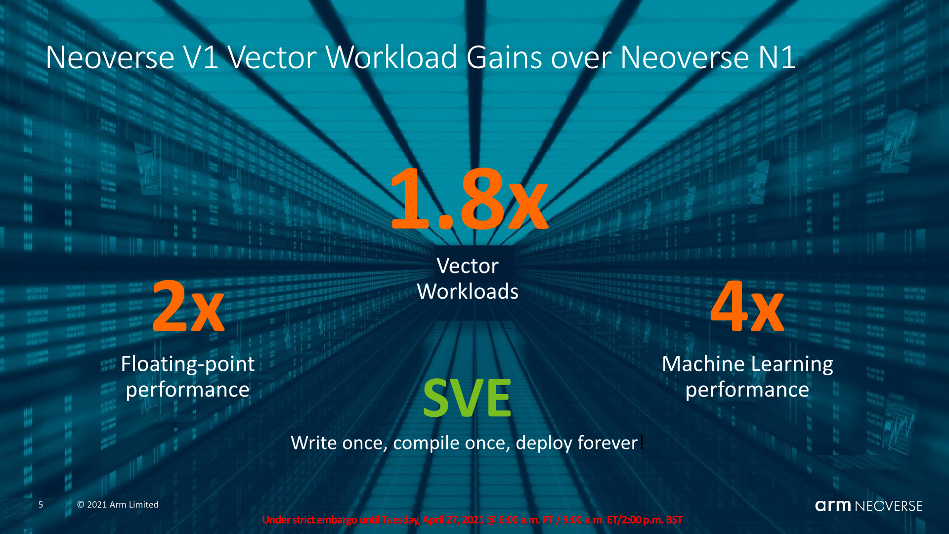

What’s clear about the Neoverse V1 is that this seems to really be an HPC-oriented design. Alongside the known SiPearl Rhea chip, backed by the European Processor Initiative’s goals for HPC uses, Korea’s ETRI (Electronics and Telecommunications Research Institute) also has a V1 designed dubbed “K-AB21” in the works, also with hybrid HBM2E and DDR5 memory. Along with today’s announcement of the V1, India’s Center for Development of Advanced Computing has also announced that they’re a V1 licensee and be using it in an exascale supercomputer project.
Essentially, it seems the V1 will serve as the foundation of many new custom HPC projects, which is a great win both for Arm as an IP vendor, as well as their licensees which are able to build something to their exact needs.
For enterprise and cloud usages, given the CPU’s power efficiency, I now doubt that we’ll somehow see implementations from cloud or merchant silicon vendors such as Amazon or Ampere, particularly because the N2 will be available.
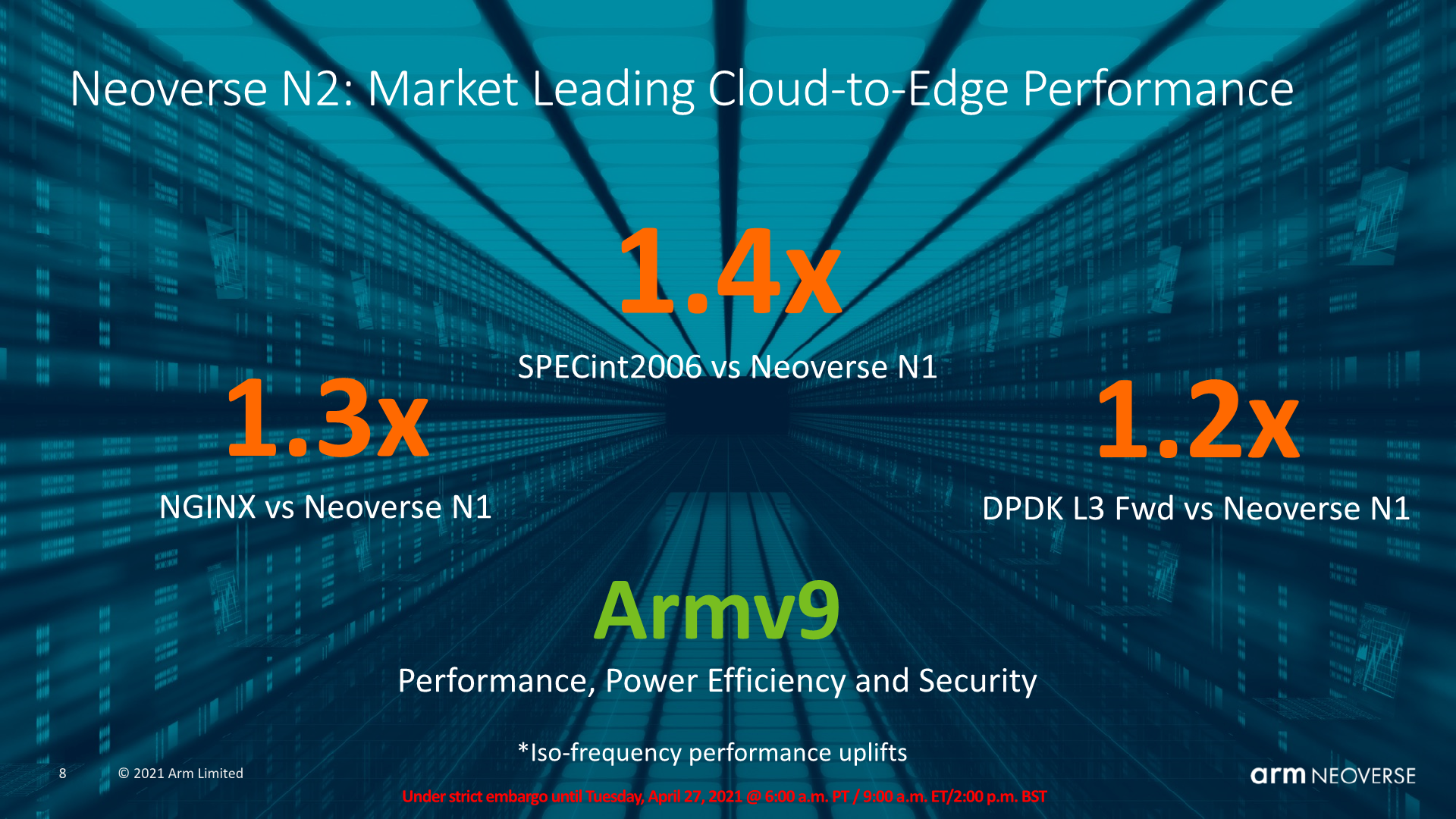
The Neoverse N2 is a more straightforward migration from the N1. IPC is improved by significant amounts which should result in good generational performance increases. I have concerns about power efficiency as the performance increases come at a linear cost of increased power. There’s a one-time opportunity to increase performance in many workloads by closing the power-gap for workloads which do not fully fill the TDP of a system today (while throttling others), however any further performance increases beyond that are dependent on actual good physical implementations by the vendors to fully take advantage of the next-generation process nodes and to execute on those theoretical gains. We’ll see how that will pan out – for now I’ll give the Arm the benefit of doubt, however we’ll also see similar gains in 5nm designs from the likes of AMD. How the competitive situation will end up in 2022 remains to be seen.
Arm had also made a note that while the N2 is a newer generation IP than the V1, roughly a year apart in design, the company actually expects for N2 products to come out only shortly after V1 products, sometime by end of this year. This further enforces my view that we’ll probably not see much V1 designs outside of the HPC market, and that Amazon and Ampere are likely to follow up with N2 based Gravitons and Altras. I want to be explicit here that none of the usual cloud vendors / CSPs / hyperscalers have yet officially commented on what kind of IP they'll be using in the next-generation designs.
The star of the show today was I think the CMN-700, and the vast new flexibility it allows vendors to achieve. The new architectural improvements and the move towards CCIX 2.0 and CXL are definitive big advances that will allow licensees to create more exotic designs. At the very least, it allows for effective usage of chiplet architecture designs, which is a much-needed feature that vendors need to adopt to be able to ensure affordability and manufacturability of products on leading edge nodes.
I’ll be looking forward to new V1 and N2 designs in 2022, and hope we’ll hear more details from licensees through the course of the year.


95 Comments
View All Comments
mode_13h - Wednesday, April 28, 2021 - link
Ah, yes! wikichip says of Zen 1:> Accordingly the peak throughput is four SSE/AVX-128 instructions
> or two AVX-256 instructions per cycle.
And Zen 2:
> This improvement doubles the peak throughput of AVX-256 instructions to four per cycle
Wow!
mode_13h - Tuesday, April 27, 2021 - link
What's SLC? I figured it was Second-Level Cache, until I saw the slide referencing "SLC -> L2 traffic"."System Level Cache", maybe? Could it be the term they use instead of L3 or LLC?
Thala - Tuesday, April 27, 2021 - link
I think you are totally right - SLC == LLC.Thala - Tuesday, April 27, 2021 - link
Quick addition. The term SLC is more popular lately, as it emphasize that the cache is not only shared among the cores but also with the system (GPU, DMAs etc).mode_13h - Wednesday, April 28, 2021 - link
Thanks. I guess I should've just waited until I'd finished reading it, because the interconnect slide made it abundantly clear.Now, I'm wondering about this "snoop filter" and why so much RAM is needed for it, when Graviton 2 & Altra have so little SLC. So, I gather it's not like tag RAM, then? Does it index the L2 of the adjacent cores, or something like that?
mode_13h - Tuesday, April 27, 2021 - link
Question and corrections on Page 6: PPA & ISO Performance ProjectionsWhat do the colors on the chip plots mean?
> Only losing out 10% IPC versus the N1
I'm sure that's meant to say "V1".
> In terms of absolute IPC improvements
Huh? These are definitely "relative IPC improvements" or just "IPC improvements".
Calin - Wednesday, April 28, 2021 - link
AWS share by vendor type: It should have been "Vendor A" and "Vendor I"mode_13h - Wednesday, April 28, 2021 - link
That slide was provided by ARM and I think they're trying to have at least the *appearance* of maintaining anonymity, even if the identities are abundantly clear.Also, you realize that their Vendor A is your Vendor I, right?
serendip - Wednesday, April 28, 2021 - link
How does the narrower front end and shallower pipeline of the N2 compare to Apple's M1? I'm thinking about how this could translate to the A78 successor, if that uses an evolution of the X1 core with improvements from N2 brought in.mode_13h - Thursday, April 29, 2021 - link
Good point. It suggests the A78+1 will perform < N2.Although, a derivative X-core would likely be > N2.