Arm Announces Neoverse V1, N2 Platforms & CPUs, CMN-700 Mesh: More Performance, More Cores, More Flexibility
by Andrei Frumusanu on April 27, 2021 9:00 AM EST- Posted in
- CPUs
- Arm
- Servers
- Infrastructure
- Neoverse N1
- Neoverse V1
- Neoverse N2
- CMN-700
PPA & ISO Performance Projections
We’ve noted about the microarchitectural changes in the new V1 and N2 processors, as well as their IPC improvements, but it’s important to actually put things into context of the actual performance and power requirements to reach those figures. Arm presented an ISO-process node figures of what we can expect out of the designs:
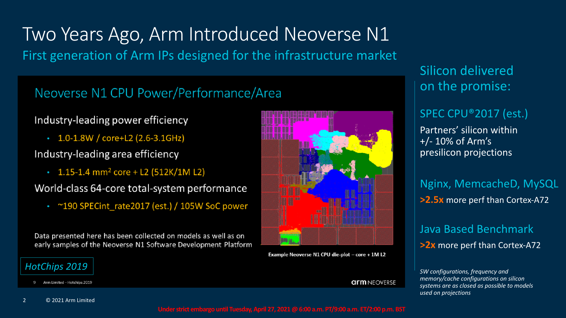
Starting off, we’re presented with a refresher of where exactly the Neoverse N1 was projected to end up. Back in 2019, the company had noted that an N1 core with 1MB L2 would take roughly 1.4mm² of area, and use up to 1.8W at 3.1GHz (TSMC 7nm node projection).
We’ve generally seen more conservative implementations (Graviton2) and more aggressive implementations (Altra Q) of the N1, but Arm states that their original presilicon projections ended up within 10% of the actual silicon performance figures of the respective products.
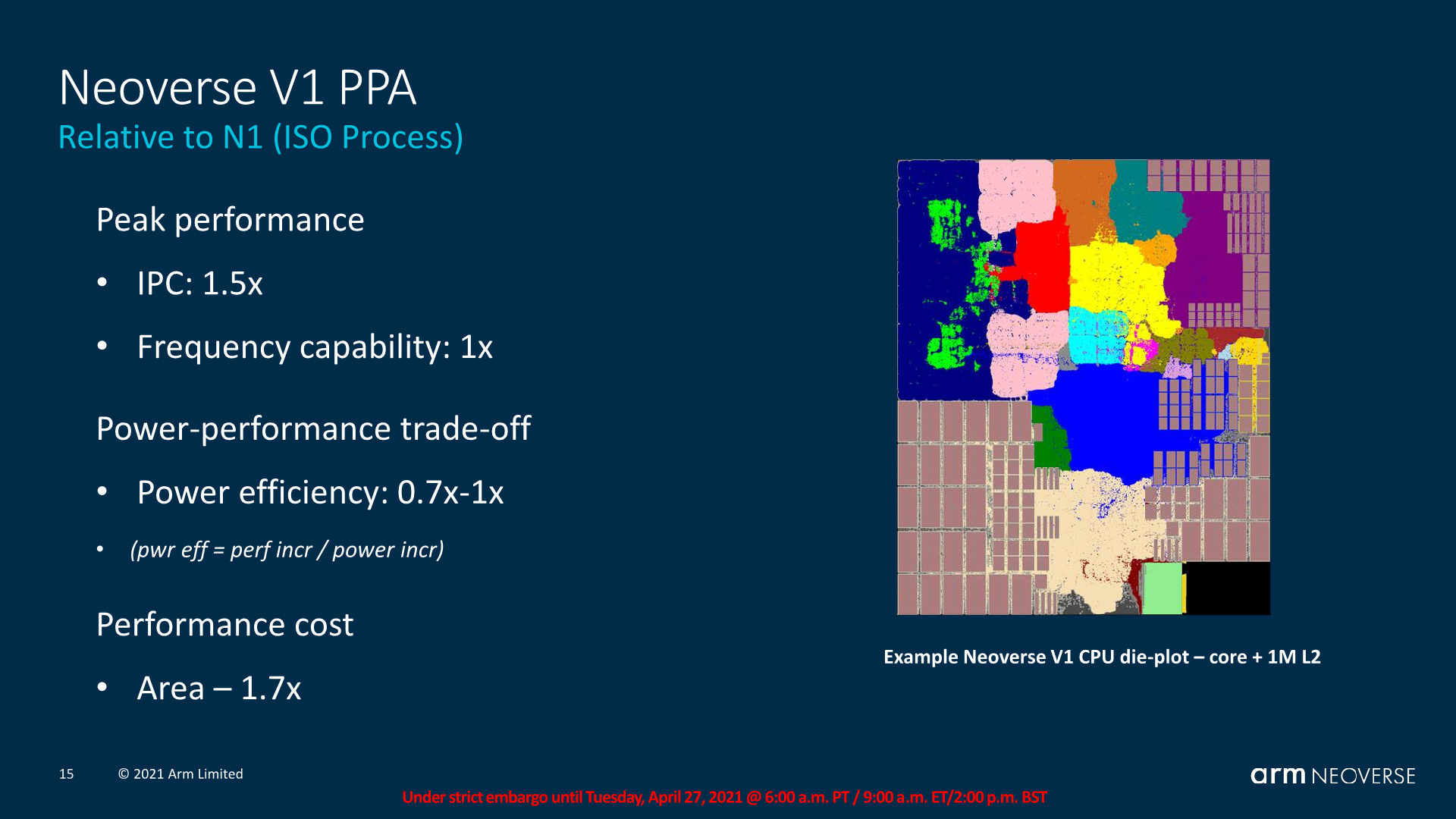
Compared to an N1, the V1 is meant to achieve 50% higher IPC, or 1.5x its predecessor while maintaining the same frequency capabilities.
What’s important to note on the slide here is that Arm is stating that power efficiency ranges from 0.7x to 1x that of the N1. Reversing the calculation for power usage increases, we actually end up with a 1.5x to 2.14x increase, which is actually quite significant. Arm also notes that the core is 1.7x larger than the N1, which is also a significant figure.
SiPearl’s Rhea chip was the first publicly known Neoverse V1 design and it features 72 cores on a N6 process node. The V1 core’s vastly increased power consumption means that it’s going to be incredibly hard to achieve similar clock frequencies while remaining in the similar 250W TDP range such as that of a current-gen top-end 80-core Altra chip, so either the core will have higher TDPs, or running at lower frequencies.
Arm also projects further non-ISO process performance figures which we’ll cover just a bit later, but there the company showcases a reference design of the V1 with 96 cores on 5nm at 2.7GHz. This means that whilst the microarchitecture seemingly would have the same frequency capabilities, the much higher power consumption of the core puts a practical limit onto the maximum frequency of any such larger core count designs.
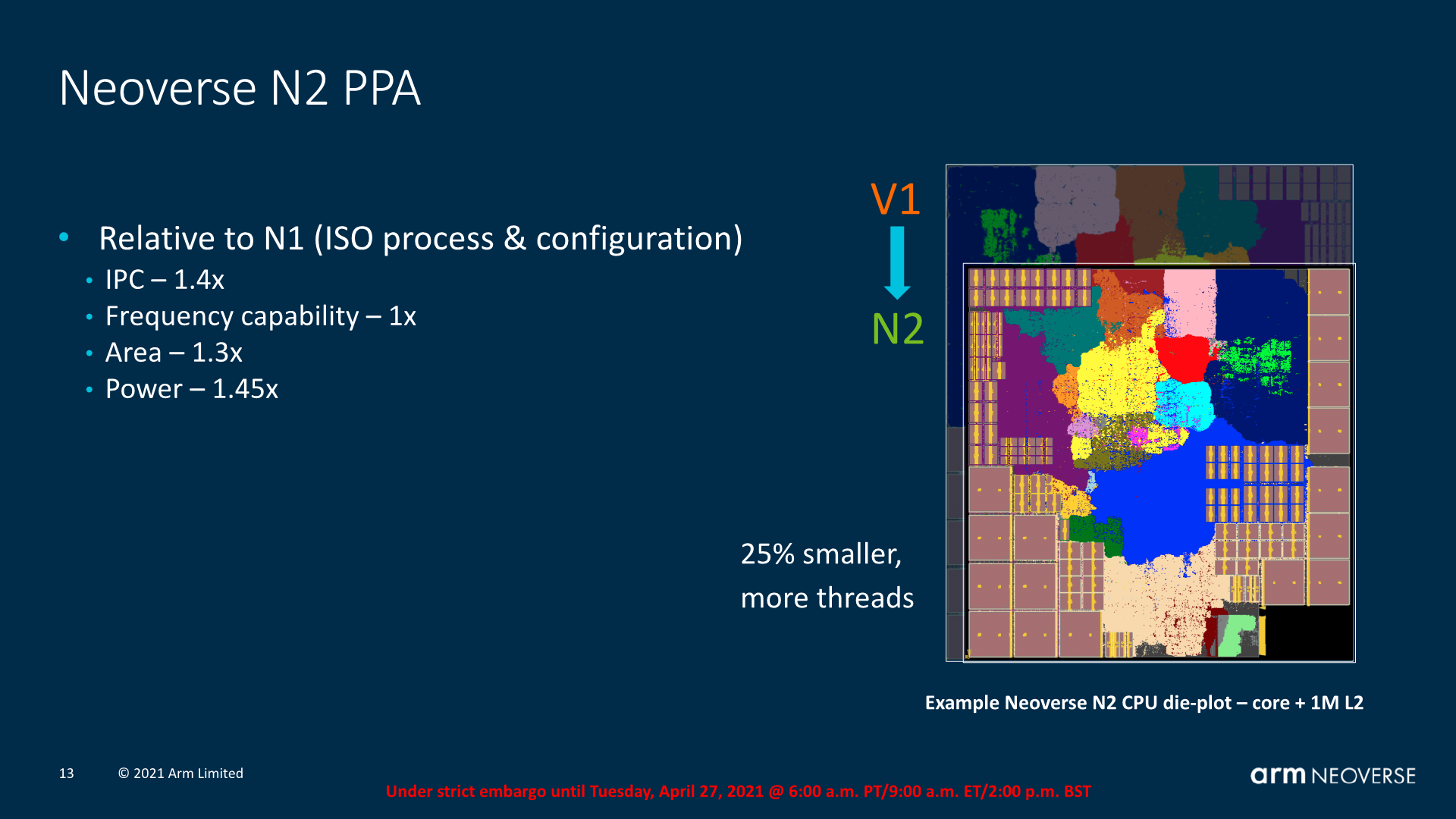
The Neoverse N2 seems a more appropriate design. Only losing out 10% IPC versus the V1, its power consumption is targeted to be only 1.45x higher than that of an N1, meaning efficiency lands in at an almost equal 96%. The area usage here is also only 1.3x that of an N1.
So generally speaking, the N2 seems to be a linear increase in performance over the N1 – both in performance and power. While this is not a regression in efficiency (well a small one at least), it does actually mean that in terms of frequency and end-performance targets, new N2 designs require larger generational process node improvements for actual vendors to be able to actually achieve the larger IPC and performance improvements that the new microarchitectures are promising.
I take note again of situations and workloads on the Ampere Altra where we’ve seen that there’s lots of workloads where the chip operates at below the TDP because the CPUs are underutilised. If an N2 design would be able to raise performance in such workloads, and more heavily throttle itself in higher demanding high utilisation workloads, it would still mean a net positive performance benefit even regardless of process node progresses. It’s a balance and situation that will be interesting to see how it plays out in eventual Neoverse N2 products.
In terms of absolute IPC improvements, Arm also disclosed a more varied set of workloads and what to expect out of the V1 and N2.
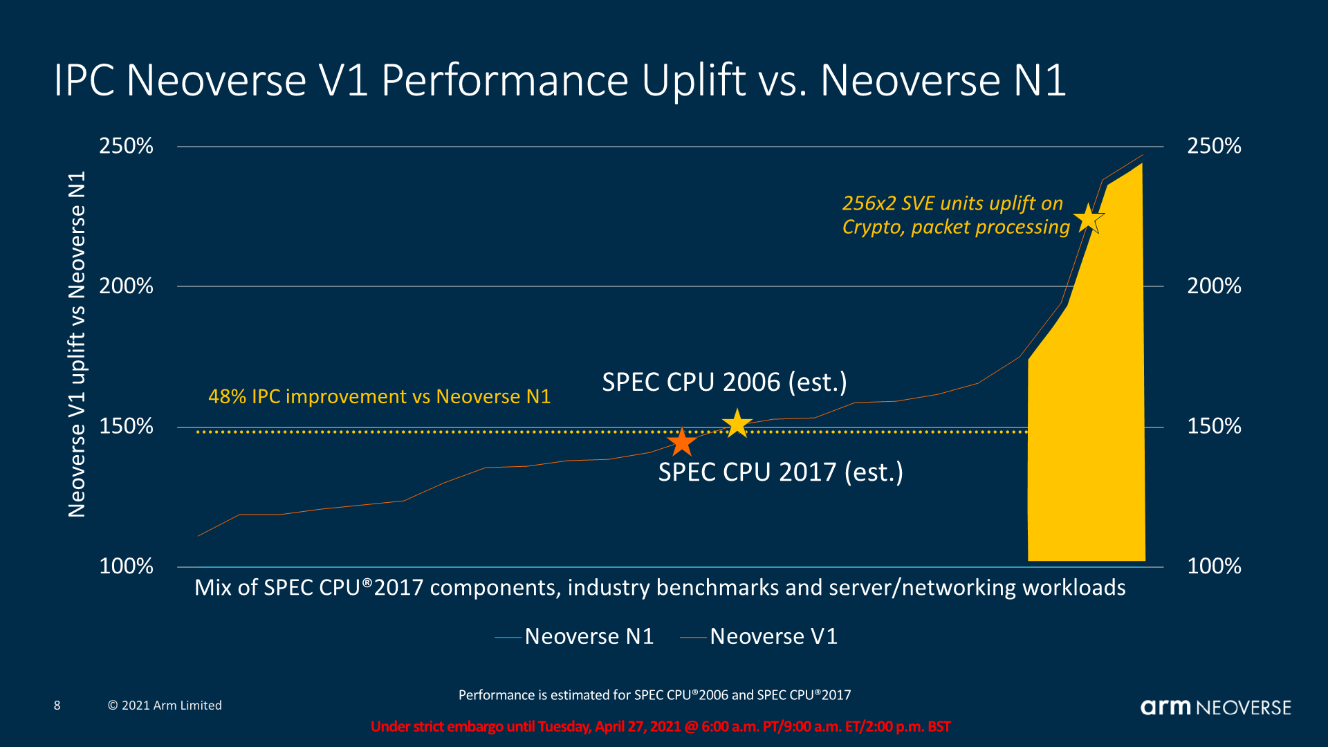
For the V1, the IPC improvements are roughly 50% median, with SPEC CPU essentially ending up at this figure. Arm made emphasis that there’s a set of workloads that are able to take advantage of SVE and the increased vector execution width of the V1 microarchitecture to achieve IPC improvements in excess of 100-125%, which is quite impressive.

The N2’s median IPC increase lands at a median of 32%, with SPEC CPU at roughly those marketed 40% figure. The high-end isn’t as high as that of the V1, but still in excess of +50% IPC.
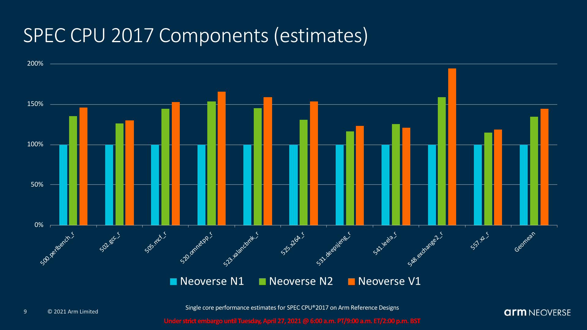
Finally, Arm also posted estimated figures for the components of SPEC CPU 2017, where we see the generational improvements be relatively even across the workloads, with a few exceptions where the V1’s larger characteristics come into play. There’s also workloads such as 541.leela_r where the N2 actually leads the V1, and Arm explained this by the fact that the N2 is actually a newer microarchitecture with further front-end improvements that aren’t found on the V1.


95 Comments
View All Comments
nandnandnand - Tuesday, April 27, 2021 - link
Looking at Cortex-X-next. It seems like Arm can put out a new Cortex-X for every new Cortex-A78 successor, since the Cortex-X is very similar but bigger.mode_13h - Tuesday, April 27, 2021 - link
Form an earlier article:> The Cortex-X1 was designed within the frame of a new program at Arm,
> which the company calls the “Cortex-X Custom Program”.
> The program is an evolution of what the company had previously
> already done with the “Built on Arm Cortex Technology” program
> released a few years ago. As a reminder, that license allowed
> customers to collaborate early in the design phase of a new
> microarchitecture, and request customizations to the configurations,
> such as a larger re-order buffer (ROB), differently tuned prefetchers,
> or interface customizations for better integrations into the SoC designs.
> Qualcomm was the predominant benefactor of this license,
Alistair - Tuesday, April 27, 2021 - link
I just want to be able to use ARM in standard DIY with an Asus motherboard and a socket, just like AMD and Intel.mode_13h - Tuesday, April 27, 2021 - link
I wonder if Nvidia will put out a Jetson-style board in something like a mini-ITX form factor.Alistair - Wednesday, April 28, 2021 - link
i sure hope so, and something not massively overpriced like right nowmode_13h - Thursday, April 29, 2021 - link
Yeah, because Nvidia is known for their bargain pricing!; )
Although, if they wanted to create a whole new product segment, it's conceivable they might keep prices rather affordable for a couple generations.
nandnandnand - Wednesday, April 28, 2021 - link
I want it. You want it. Some people seem to want it. Maybe demand is forming? Get on it, China.16-core Cortex-X2 please.
mode_13h - Wednesday, April 28, 2021 - link
They already did, sort of. See: https://e.huawei.com/us/products/servers/kunpeng/k...Whoops! Had to get this out of Google cache, because the page 404'd:
Board Model D920S10
Processors 1 Kunpeng 920 processor, 4/8 cores, 2.6 GHz
Internal Storage 6 SATA 3.0 hard drive interfaces, 2 M.2 SSD slots
Memory 4 DDR4-2666 UDIMM slots, up to 64 GB
PCIe Expansion 1 PCIe 3.0 x16, 1 PCIe 3.0 x4, and 1 PCIe 3.0 x1 slots
LOM Network Ports 2 LOM NIC, supporting GE network ports or optical ports
USB 4 USB 3.0 and 4 USB 2.0
mode_13h - Tuesday, April 27, 2021 - link
Do any of the current x86 cores pair up SSE operations for >= 4x throughput per cycle?AVX2 has been around for long enough that a lot of the code which could benefit from it has already been written to do so, yet *most* people are still compiling to baseline x86-64 (or just above that), since Intel is still making low-power cores without any AVX. So, I'm sure there's still *some* code that could benefit from >= 4x SSEn execution.
AntonErtl - Wednesday, April 28, 2021 - link
Zen has 4 128-bit FP units (2 FMA and 2 FADD). Not sure if that's what you are interested in.