Arm Announces Neoverse V1, N2 Platforms & CPUs, CMN-700 Mesh: More Performance, More Cores, More Flexibility
by Andrei Frumusanu on April 27, 2021 9:00 AM EST- Posted in
- CPUs
- Arm
- Servers
- Infrastructure
- Neoverse N1
- Neoverse V1
- Neoverse N2
- CMN-700
PPA & ISO Performance Projections
We’ve noted about the microarchitectural changes in the new V1 and N2 processors, as well as their IPC improvements, but it’s important to actually put things into context of the actual performance and power requirements to reach those figures. Arm presented an ISO-process node figures of what we can expect out of the designs:
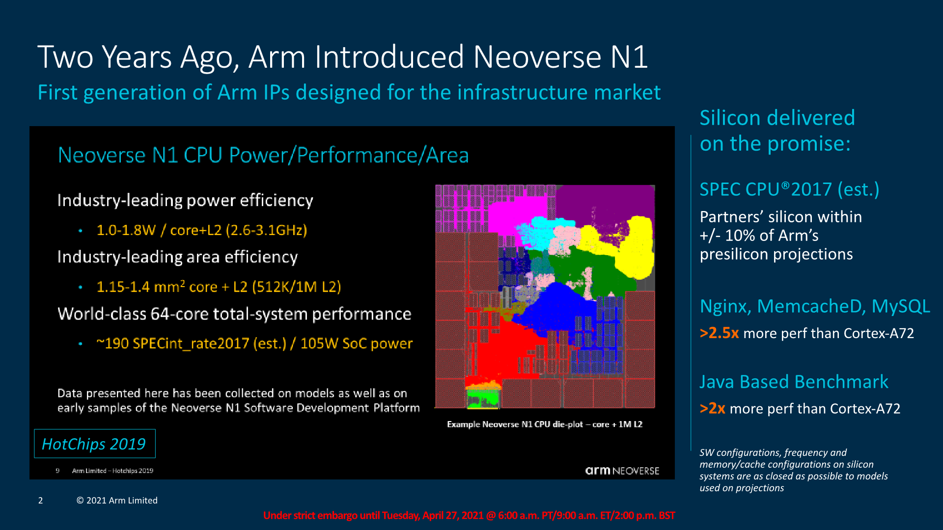
Starting off, we’re presented with a refresher of where exactly the Neoverse N1 was projected to end up. Back in 2019, the company had noted that an N1 core with 1MB L2 would take roughly 1.4mm² of area, and use up to 1.8W at 3.1GHz (TSMC 7nm node projection).
We’ve generally seen more conservative implementations (Graviton2) and more aggressive implementations (Altra Q) of the N1, but Arm states that their original presilicon projections ended up within 10% of the actual silicon performance figures of the respective products.
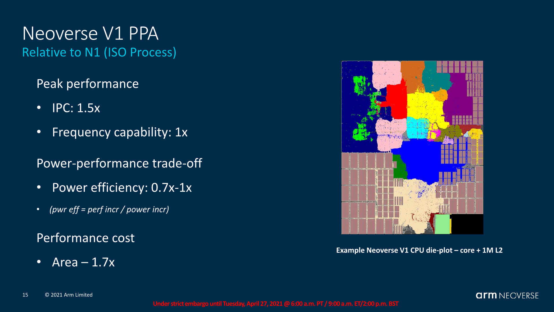
Compared to an N1, the V1 is meant to achieve 50% higher IPC, or 1.5x its predecessor while maintaining the same frequency capabilities.
What’s important to note on the slide here is that Arm is stating that power efficiency ranges from 0.7x to 1x that of the N1. Reversing the calculation for power usage increases, we actually end up with a 1.5x to 2.14x increase, which is actually quite significant. Arm also notes that the core is 1.7x larger than the N1, which is also a significant figure.
SiPearl’s Rhea chip was the first publicly known Neoverse V1 design and it features 72 cores on a N6 process node. The V1 core’s vastly increased power consumption means that it’s going to be incredibly hard to achieve similar clock frequencies while remaining in the similar 250W TDP range such as that of a current-gen top-end 80-core Altra chip, so either the core will have higher TDPs, or running at lower frequencies.
Arm also projects further non-ISO process performance figures which we’ll cover just a bit later, but there the company showcases a reference design of the V1 with 96 cores on 5nm at 2.7GHz. This means that whilst the microarchitecture seemingly would have the same frequency capabilities, the much higher power consumption of the core puts a practical limit onto the maximum frequency of any such larger core count designs.
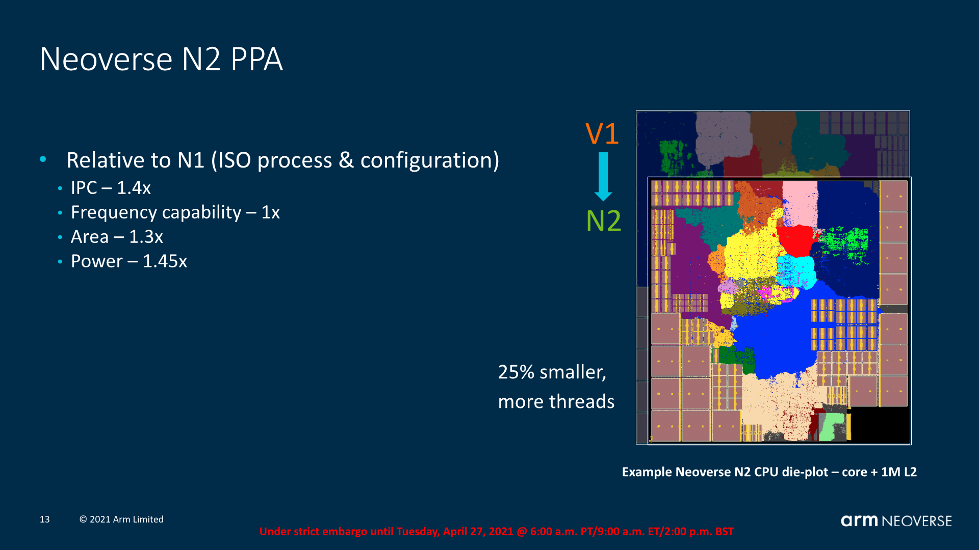
The Neoverse N2 seems a more appropriate design. Only losing out 10% IPC versus the V1, its power consumption is targeted to be only 1.45x higher than that of an N1, meaning efficiency lands in at an almost equal 96%. The area usage here is also only 1.3x that of an N1.
So generally speaking, the N2 seems to be a linear increase in performance over the N1 – both in performance and power. While this is not a regression in efficiency (well a small one at least), it does actually mean that in terms of frequency and end-performance targets, new N2 designs require larger generational process node improvements for actual vendors to be able to actually achieve the larger IPC and performance improvements that the new microarchitectures are promising.
I take note again of situations and workloads on the Ampere Altra where we’ve seen that there’s lots of workloads where the chip operates at below the TDP because the CPUs are underutilised. If an N2 design would be able to raise performance in such workloads, and more heavily throttle itself in higher demanding high utilisation workloads, it would still mean a net positive performance benefit even regardless of process node progresses. It’s a balance and situation that will be interesting to see how it plays out in eventual Neoverse N2 products.
In terms of absolute IPC improvements, Arm also disclosed a more varied set of workloads and what to expect out of the V1 and N2.
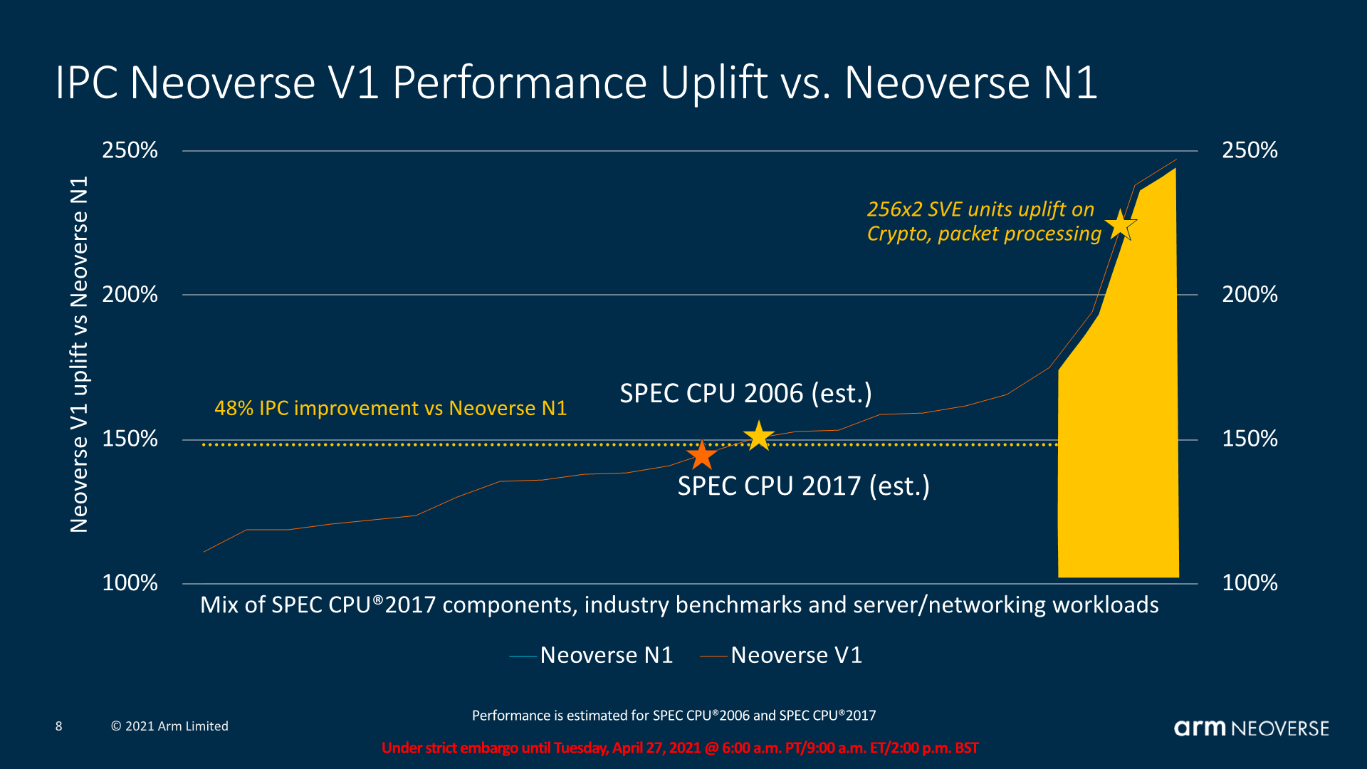
For the V1, the IPC improvements are roughly 50% median, with SPEC CPU essentially ending up at this figure. Arm made emphasis that there’s a set of workloads that are able to take advantage of SVE and the increased vector execution width of the V1 microarchitecture to achieve IPC improvements in excess of 100-125%, which is quite impressive.

The N2’s median IPC increase lands at a median of 32%, with SPEC CPU at roughly those marketed 40% figure. The high-end isn’t as high as that of the V1, but still in excess of +50% IPC.
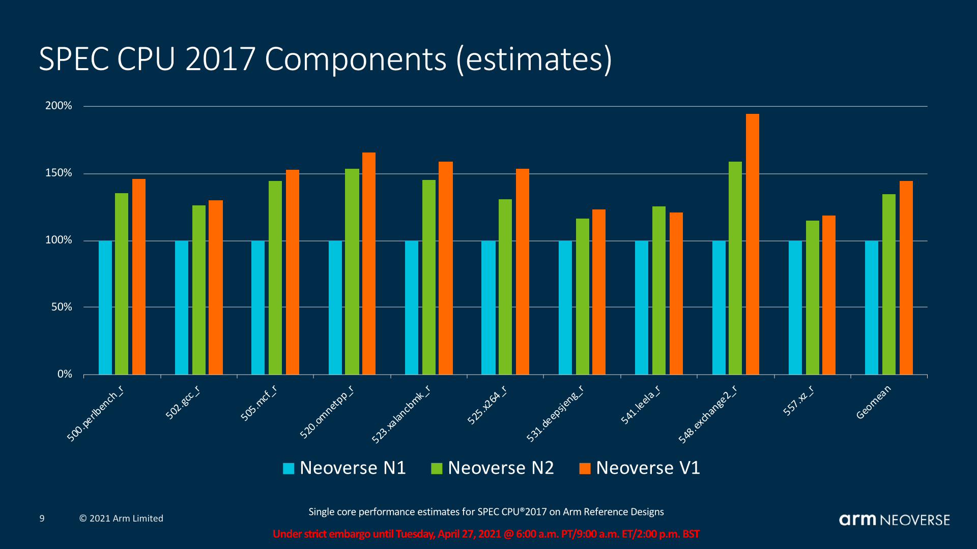
Finally, Arm also posted estimated figures for the components of SPEC CPU 2017, where we see the generational improvements be relatively even across the workloads, with a few exceptions where the V1’s larger characteristics come into play. There’s also workloads such as 541.leela_r where the N2 actually leads the V1, and Arm explained this by the fact that the N2 is actually a newer microarchitecture with further front-end improvements that aren’t found on the V1.


95 Comments
View All Comments
yeeeeman - Tuesday, April 27, 2021 - link
what about a cortex a55 successor?SarahKerrigan - Tuesday, April 27, 2021 - link
I'd expect to see one next month launching alongside Matterhorn.eastcoast_pete - Tuesday, April 27, 2021 - link
Hi Sarah, can you post any links (including rumors) about that? Given ARM's focus on bigger, high performance-oriented designs, the LITTLE cores haven't gotten a lot of love in recent years. The persistence of the in-order designs for ARM LITTLE cores is one of the reasons why I find the dominance of ARM troubling; that clearly stood still because there is nowhere else to turn to for many, i.e. they didn't have to change it. In x86, at least we have two larger players having their own, yet compatible designs.SarahKerrigan - Tuesday, April 27, 2021 - link
I've seen it reported in a few places, including on RWT which is a pain to search - but since task migration generally requires compatible instruction sets between big and little cores, it's pretty clear that Matterhorn will bring a small, low-power friend when it arrives.Raqia - Tuesday, April 27, 2021 - link
I wonder if they could simply repurpose either a refresh of the A73 or A75 as the little core. Surely with the new fabrication processes available, die area relative to a big Matterhorn core should be comparable to A55 vs A78/X1, but the question becomes performance / energy. Integer performance of A75/73 vs. Ice Storm is comparable with the former winning by a bit in FP, but efficiency is light years apart:https://images.anandtech.com/doci/13614/SPEC-perf-...
https://images.anandtech.com/doci/16192/spec2006_A...
SarahKerrigan - Tuesday, April 27, 2021 - link
I think use of a refreshed A65 without multithreading and with the new ops seems more plausible to me.Raqia - Tuesday, April 27, 2021 - link
That could make sense; there's fairly little information on the micro-architecture of the A65 or A65AE at present except that it does do OoOE, and it's unclear what clocks and efficiency it can achieve as well:https://developer.arm.com/documentation/100439/010...
It does sport a bigger maximum L2 configuration than the A55. They do need to up their game here as the A55 makes a pretty poor showing for efficiency compared to Apple's small core (which got even worse in the A14 generation):
https://images.anandtech.com/doci/14072/SPEC2006ef...
At least wattage and hence current draw is low.
SarahKerrigan - Tuesday, April 27, 2021 - link
A65 is E1, which has had a uarch dive on this site.Raqia - Wednesday, April 28, 2021 - link
Got it, thanks for that! The A65 is interesting, without SMT they are quoting a pretty modest bump in integer performance < 20% at a bit more than half the power of A55 at 7nm:https://images.anandtech.com/doci/13959/07_Infra%2...
https://images.anandtech.com/doci/13959/07_Infra%2...
They could probably tune this to be better without SMT, but are you against having SMT for security reasons?
It's still not close to Apple's small cores in performance, but efficiency might be in the same ballpark now. ARM designs are quite good in terms of PPA but even their performance oriented X1 is likely only 70% the die area as a Firestorm core, and their cache hierarchies are more complex as core designs pull double duty for servers parts too.
It probably made sense to have fewer transistors per CPU core as quite a few Android SoC vendors integrated modems on die, but this may change once Qualcomm digests its Nuvia purchase and move to a smaller node. All parties may hit a wall for per core improvements as slowing SRAM density improvements at new nodes bottleneck what gains are gotten from logic density improvements.
Kangal - Thursday, April 29, 2021 - link
TL;DR - ARM needs to focus on a new product stack. It needs to have a diverse ARMv9 lineup of small, medium, large chipset options. With the small chipset being very scalable down to Tiny IoT Sensor level. Whereas the large chipset being scalable up to large supercomputers and servers. Whilst the medium chipset focusing on phones and tablets. As this covers full SoC, it includes both CPUs and GPUs.Long version:
I know making these architectures is a huge challenge, but ARM has been a little lazy in some scenarios. I know they're basically following the money in the industry, and that means chasing the "phablet" market for CPUs and GPUs. But they've been leaving themselves vulnerable to gaps, in either smaller power or larger power systems, that can be exploited by competitors, such as RISC-V. If not, even x86 might poke some wins here and there.
Ages ago, like 2013, they had the A7 (tiny), A15 (small), and A57 (medium) core designs. Basically covering most bases. Along with the Mali-400 iGPU, and 1GB-2GB Shared-RAM, to do some compute tasks. To say ARM was innovative would be a disservice to the technology they brought forward. That's in contrast to x86 Intel's Atom (small) and Intel's Core-i7Y/M (large), as well as Intel Iris Pro iGPU with 8GB Shared-RAM in systems of the time. Then ARM made the leap into 64bit processing around 2016. The lineup evolved into the A35 (tiny), A53 (small), A73 (medium) core designs, running with 1GB-2GB-4GB sRAM, and used modest G31 (tiny) to G51 (small) to G71 (medium) iGPU options. Again, this lineup was very innovative and impressive. Contrast that to the new x86 competition in AMD's 16nm Vega Large-iGPU, and Zen1 Large-CPU.
However... There hasn't been any upgrades for the "tiny" portfolio, being stuck to the offerings of Cortex A35 CPU and G31 GPU ever since. There has been only a slight refresh to the "small" portfolio, upgrading to the Cortex A55 CPU, and the G52 and G57 iGPUs. To the point that they're a joke, and easily surpassable by the competitors. ARM really needs a revolutionary new design here, it needs to be super-efficient. Perhaps something that can scale between both tiny and small categories: with performance ranging from the A55 (or more) at the "tiny" power-level, to the A73 (or more) at the "small" power-level. Basically catching up to Apple, if unable to surpass them.
Whereas the "medium" portfolio has seen very frequent upgrades, in the CPU-side to the Cortex A75, A76, A77, and A78. In the GPU-side we've seen G72, G76, G77, G78 which have been mostly competitive, surpassing some custom implementations (Samsung/MediaTek) and losing to others (Apple/Qualcomm). Not much needs to change here to be honest. We've also seen the emergence of a new "large" category of ARM processors. Firstly popularised by custom implementations from Apple (A10 and onwards), then Samsung (Mongoose M3, and onwards). Now it's supported officially by ARM in the form of the Cortex A77+ and the Cortex A78X / X1. This has been mostly underwhelming and uncompetitive, with Apple being the only one implementing good designs. There hasn't been any new "large" category for iGPUs from ARM or competitors, with the only Large-iGPU exception actually being inside the Apple Silicon M1. ARM (without counting Apple) needs to do better here, and it looks like ARM might already be focussing here in the future with ARMv9. Again contrast this to the x86 markets offering 7nm Large-CPUs of Zen2 and Zen3, with RDNA-1 and RDNA-2 Large-GPUs.