Qualcomm Details The Snapdragon 888: 3rd Gen 5G & Cortex-X1 on 5nm
by Andrei Frumusanu on December 2, 2020 10:00 AM EST- Posted in
- Mobile
- Qualcomm
- Smartphones
- SoCs
- 5G
- Cortex A78
- Cortex X1
- Snapdragon 888
Hexagon 780: A Whole new IP for AI & DSP
Every year Qualcomm likes to talk about its new Hexagon DSPs, with the last few generations also adding to the table new Tensor Accelerators dedicated for ML inferencing. This year’s Snapdragon 888 design also hypes up the new Hexagon 780 design, with the difference being that this time around the generational improvements are truly humongous.

The new Hexagon 780 accelerator IP truly deserves a large increment in its IP numbering scheme, as it’s essentially a ground-up redesign of the company’s existing DSP with scalar and vector execution engines, and the recent Tensor Accelerators. Previously all these execution engines were acting as discrete independent blocks within the Hexagon 600 series family, but that’s now changed in the new IP design.
The new IP block fuses together all the scalar, tensor, and vector capabilities into a single monolithic IP, vastly increasing the performance and power efficiency of workloads that make a use of all the mixed capabilities of the design.
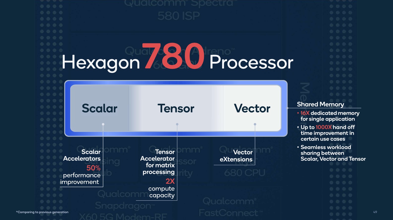
In terms of performance uplifts, scalar execution capabilities are said to be increased by 50%, while tensor execution throughput has doubled. The vector extension units seem to have remained the same this generation, but actual performance of workloads will still have been increased thanks to the new memory architecture of the new IP block.
Qualcomm states that they’ve increased the on-chip SRAM dedicated to the block 16-fold, allowing for larger machine-learning inference models to fit within the block’s memory, greatly accelerating their performance. This larger memory pool also allows for coherency between the scalar, vector and tensor units, allowing for the vastly increased workload handoff time between the different execution engines. I asked about the actual size of this new memory, but the company wouldn’t disclose any further details, just stating that it’s significant.
The company’s engineers were extremely hyped up about the new design, stating that the performance and flexibility of the new design is well beyond that of what other companies can achieve through disaggregated DSP and ML inference engines, sometimes even from different IP vendors.
The most important figure for the new design is the 3x performance per watt claim, which is just a massive generational improvement that you rarely see in the industry.

As is usual for Qualcomm, the company doesn’t actually state the per-block performance increases, but instead opts to showcase an aggregate computational throughput figure shared amongst all of the SoC’s IP blocks, including CPU, GPU, and the new Hexagon accelerator block. This new figure lands in at 26TOPs for the Snapdragon 888, which is 73% higher than the 15TOPs figure of the Snapdragon 865. Given that we’ve seen significant changes in all IP blocks this generation, I won’t attempt a breakdown estimate as it’s likely going to be wrong and off-the-mark anyhow.
The Adreno 660 - A 35% faster GPU
Amongst the improvements which lead up to that 26TOPs figure is a new vastly improved GPU in the form of the new Adreno 660.
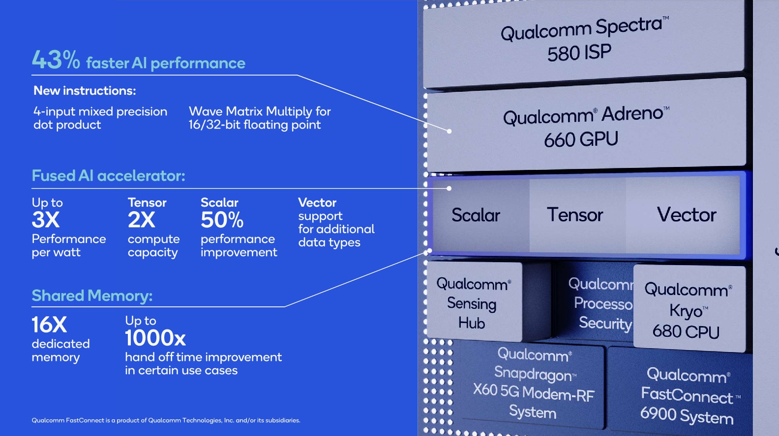
Qualcomm still holds architectural details of their GPUs very close to their chest and thus doesn’t go disclose very much about the new GPU design and what has actually changed, but one thing they did talk about is the addition of new mixed-precision dot product as well as FP16/FP32 wave matrix-multiply instructions, which allow the new GPU to increase AI performance by up to 43%.
We’re also seeing the addition of variable rate shading (VRS) onto the Adreno GPU architecture, allowing for coarser pixel shading onto larger pixel blocks for object and screen areas which don’t require as much detail or the native resolution shading wouldn’t be noticeable. This is also a major feature that’s being introduced in the console and new-generation PC graphics cards and GPUs, which should bring greater performance uplift for new gaming titles which take advantage of the new features. It’s great to see Qualcomm bringing this to the mobile space along with the rest of the industry.
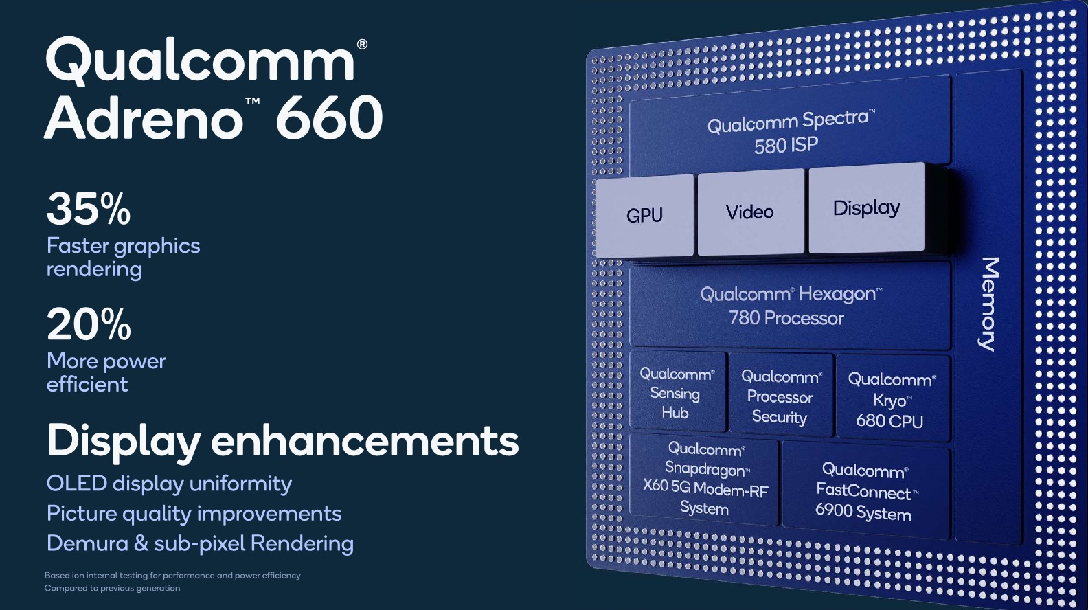
For graphics workloads, the new GPU is advertised as being able to increase performance by up to 35%, which is a very major generational performance leap.
Such a performance jump would actually signify that Qualcomm may very well regain the gaming performance crown this generation, having lost it to Apple’s SoCs over the last two generations. Apple’s latest A14 has seen rather conservative gains on the GPU side this year, so a 35% performance gain over the Snapdragon 865 should very much allow the new Snapdragon 888 to retake the leadership position.
A 35% performance increase with a 20% power efficiency increase would indicate that the new SoC would achieve the higher performance at cost of a little higher power consumption, but given the Snapdragon 865’s excellent power characteristics of below 4W, Qualcomm does have a little leeway to increase power this generation.
3200MHz LPDDR5
The new Snapdragon 888 moves from a hybrid memory controller to one that focuses on LPDDR5, and also increases the frequency support for new LPDDR5 to 3200MHz (Or LPDDR5-6400).
For the Snapdragon 865 Qualcomm was rather unenthusiastic about the LPDDR5 switch, saying that it didn’t bring all to great improvements to performance or power efficiency – something which we actually did test out and come to the same conclusion in our review of the two OnePlus 8 phones, where the LPDDR4X variant ended up being no slower and seemingly actually more efficient to us. Apple this year also kept on using LPDDR4X on their A14 and M1 SoCs – pointing out that the benefits aren’t all that great.
For the Snadpragon 888 however, Qualcomm’s engineers seemed more upbeat about LPDDR5 and the new SoC actually being able to utilise the increase memory bandwidth this generation. Without going into details, the company also stated that they’ve improved the overall design of the memory subsystem, improving aspects such as latency.
On the part of the memory subsystem, Qualcomm still employs a 3MB system-level-cache in front of the memory controllers, with the ability of all SoC IP blocks to take advantage of this cache.


123 Comments
View All Comments
ZolaIII - Wednesday, December 2, 2020 - link
Well based on the QC claims, 20% more power efficient = same number of GPU clusters and same alignment as the power saving is from process improvement, they made a new pipeline to include additional functions but fundamental blocks remain unchanged (actually ALU's didn't change from Ati days).This is just based on my assumptions and logic. Upon which I don't think it's enough to be stated as new gen.
I don't have problem with numerology including additional make believes tied to the name change, at least that's not a snake oil like the rest.
Given in mind rest of the story (trade wars) actually the QC naming thing is pathetic.
Who ever makes a real flagship SoC (not saying on the die size), even if based on reference IP's based upon 5 nm TSMC has the opportunity to rip this abomination without to much hustle.
Raqia - Wednesday, December 2, 2020 - link
Transistor count and die size haven't been revealed yet; I have my doubts many other companies could integrate all those subsystems with the PPA that Qualcomm achieves. Even Apple doesn't get there as they don't integrate a modem which is far far trickier than you might expect.ZolaIII - Wednesday, December 2, 2020 - link
Well you are right about that (modem, RF and cetera) and thing's won't get better any time soon, call it democracy.Rest is IP license available. If you raise a bar to actual manufacturers (in their own menagement) list goes to none as ironically Samsung is by far most adequate. I guess things will get boring until GAA.
melgross - Wednesday, December 2, 2020 - link
Apple hasn’t been allowed to integrate a modem. It’s likely that a major reason they bought Intel’s work is so that they can have their own, so that they can do that. But Apple seems to have no problems with efficiency, even with an external modem. I suspect that it’s the Android OSs known efficiency problems, among others, such as the requirement for double the RAM, that’s causing these problems, which is why those phones require batteries that are so much larger.Raqia - Wednesday, December 2, 2020 - link
It's a fallacy that an external modem is any less power efficient than an on SoC one, and in fact fab process can be further optimized for a totally separate modem die which really does have different requirements than CPUs and GPUs. The reason Qualcomm, Samsung, Mediatek and Huawei do it is to reduce cost and complexity. Apple simply doesn't the IP necessary and the purchase of Intel's money losing unit was primarily for IP, some talent rather than design or implementation; it still won't get them a competitive modem in house for several years to come.ZolaIII - Thursday, December 3, 2020 - link
It's a fact how it isn't a one peace to start with. RF analog-mixed part & processesing part which can be integrated. RF part didn't progress regarding it's manufacturing processes in very, very long time & in best case scenario is built upon SOI. In the world of mobile SoC high density libs are commonly used for everything already (excluding analogue, MOSFET's and cetera of course).KusheYemi - Wednesday, December 2, 2020 - link
Qualcomm updated their processor the right way. They improved all of the main day to day functions that ordinary people use frequently. Tech savvy people might be disappointed about the raw compute power but the SD865 was already great.halcyon - Wednesday, December 2, 2020 - link
If they wanted to improve the day-to-day, they would have made it much more power efficient and replaced those ageing A55 cores that are used for mosts daily simple tasks.melgross - Wednesday, December 2, 2020 - link
Great compared to what, other mediocre SoCs?The Hardcard - Wednesday, December 2, 2020 - link
I don’t know why people only see great or horrible with nothing in between. This is a good competitive chip - only people desperately aching for someone to overtake Apple can be seriously disappointed.The single X1 is a solution to having good singlethread speed and the UI responsiveness that comes with that while giving good multicore combined with efficiency. Is it the best solution? I don’t know, but it’s not a bad one.
The clock speed is interesting however. I have to think that there are process limitations there. ARM targeted 3 GHz, which would’ve given it some floating point wins over the A13 based on Andrei‘s estimates. The 5% shortfall will put them pretty squarely behind the A13, I’m sure they wouldn’t have excepted that unless they had no choice.