Qualcomm Details The Snapdragon 888: 3rd Gen 5G & Cortex-X1 on 5nm
by Andrei Frumusanu on December 2, 2020 10:00 AM EST- Posted in
- Mobile
- Qualcomm
- Smartphones
- SoCs
- 5G
- Cortex A78
- Cortex X1
- Snapdragon 888
Conclusion & First Impressions
The new Snapdragon 888 is overall a very impressive package from Qualcomm, advancing the most important areas for which today’s smartphones are being used. 5G connectivity was the big new feature of 2020 SoCs and smartphones, and the new 888 platform represents the evolution and maturing of the new technologies that had been introduced in prior generations.
The big focus point of the Snapdragon 888 were clearly AI and cameras. The new Hexagon 780 IP block looks immensely impressive and to me seems like a major competitive advantage of the new SoC design – other vendors which aren’t as vertically integrated with their accelerator IPs will have to respond to Qualcomm’s new advancements as it seems like a major performance advantage that will be hard to mimic.
Today’s flagship smartphones have diminished ways of differentiating themselves from one another, with the cameras still being the one aspect where vendors still have very different approaches to their designs. Qualcomm’s push for a triple-ISP system in the Snapdragon 888 pushes the upper limits of what vendors will be able to do on their smartphones, allowing for a continued push for the smartphone camera ecosystem. Even for still-picture camera experiences, it seems that Qualcomm is expecting a more notable technology jump in 2021 as we see the introduction of new sensors and imaging techniques, enabled by the new SoC.
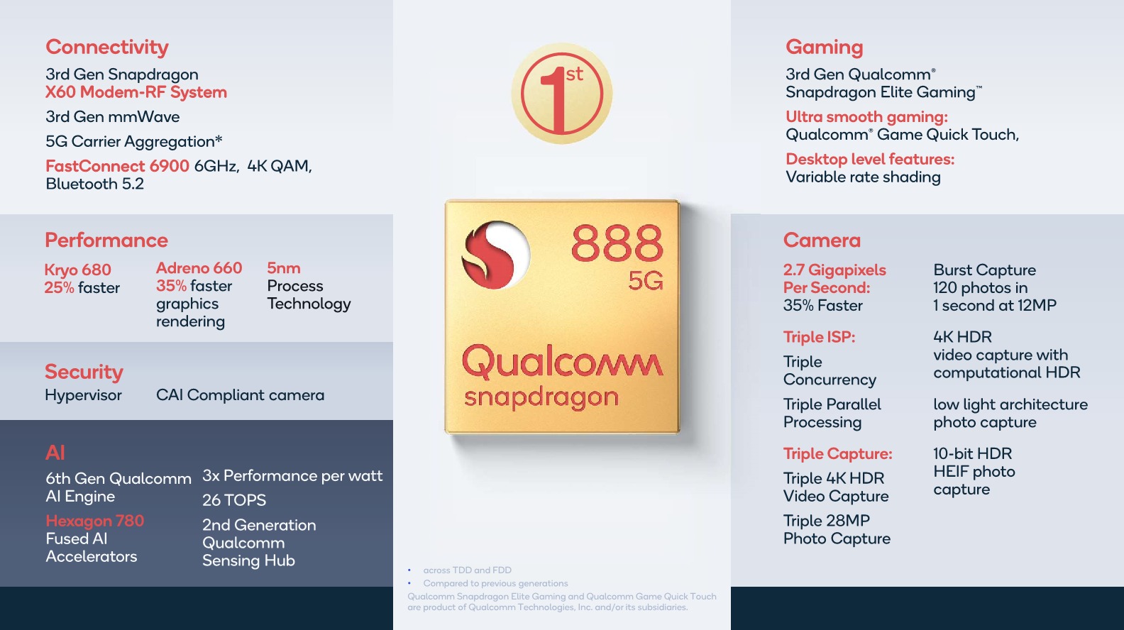
The new CPU configuration gives the new SoC a good uplift in performance, although it’s admittedly less of a jump than I had hoped for this generation of Cortex-X1 designs, and I do think Qualcomm won’t be able to retain the performance crown for this generation of Android-SoCs, with the performance gap against Apple’s SoCs also narrowing less than we had hoped for.
On the GPU side, the new 35% performance uplift is extremely impressive. If Qualcomm is really able to maintain similar power figures this generation, it should allow the Snapdragon 888 to retake the performance crown in mobile, and actually retain it for the majority of 2021.
The new Snapdragon 888 to me looks like a continuation of Qualcomm’s excellent execution over the last few years. Striking a balance between performance, power efficiency, and features is something that may be harder than it sounds, and Qualcomm’s engineering teams here seem to be focused on being able to deliver the overall best package.
Much like the Snapdragon 865, and the last couple of generations of Snapdragon SoCs before it, I expect the new Snapdragon 888 to be an excellent foundation for 2021’s flagship devices, and I’m looking forward to experience the new generation.
Related Reading:
- Qualcomm Tech Summit 2020: Day One LiveBlog (10:00 ET, 15:00 UTC)
- Qualcomm’s New 3rd Generation Snapdragon X60 5G Modem, Built on 5nm
- Qualcomm Announces Snapdragon 865+: Breaking the 3GHz Threshold
- The Snapdragon 865 Performance Preview: Setting the Stage for Flagship Android 2020
- Qualcomm Announces Snapdragon 865 and 765(G): 5G For All in 2020, All The Details
- The Snapdragon 855 Performance Preview: Setting the Stage for Flagship Android 2019
- The Qualcomm Snapdragon 855 Pre-Dive: Going Into Detail on 2019's Flagship Android SoC


123 Comments
View All Comments
iphonebestgamephone - Sunday, December 6, 2020 - link
Mediatek gonna trash qualcomm this year!!ChrisGX - Sunday, December 13, 2020 - link
7FFP has the same density as 7FF but has a number of improvements. The dense TSMC process is 7FF+ (also known as N7+) and it is an EUV node. The dense node you refer to is 7FF+. Somebody seems to have wrongly assumed that P refers to plus - it doesn't. Still, the error after exchange by many hands has become pervasive on the web.EMMVIN - Thursday, December 3, 2020 - link
When can we expect the detailed analysis of the soc and benchmark comparisons. There is nothing out there that is as detailed as yours. Hope you guys already have an early sample to test :)tuxRoller - Friday, December 4, 2020 - link
I'm curious if the move to samsung negatively affected clocking. If not, then this is a really cheap move in favor of their later 888+.vladx - Friday, December 4, 2020 - link
Still no AV1 decoding at least? Pathetic from QualcommJames5mith - Saturday, December 5, 2020 - link
"allowing for the vastly increased workload handoff time between the different execution engines"So it's much slower now?
peevee - Thursday, December 10, 2020 - link
"multi-frame noise reduction engines inside of the ISPs. It’s said that the quality of the noise reduction has been improved this generation, allowing for even better low-light captures with the native capture mode (no computational photography)"What you have described IS computational photography.
KarlKastor - Saturday, December 12, 2020 - link
@AndreiI can't really understand, where you see the 7LPP in a disadvantage in comparison to N7.
If you compare the 765G with the middle cores of the 855, you see similar power draw.
The comparison to the Kirin show higher frequency and higher power for the Kirin. I can't see a winner here. You can't look at the efficiency score. The performance is higher with the Kirin because of the bigger Caches. Double the L2 and 4x L3. Memory bandwidth and SL-Cache is bigger too.
ChrisGX - Sunday, December 13, 2020 - link
You have a point in connection to the N7 but you are on shakier ground with regard to the N7P and N7+. The Semiwiki article shows the density advantage of N7+ process (otherwise known as 7FF+ and mislabelled in the article as 7FFP) used on the Kirin 990 5G SoC. TSMC data likewise underscores the greater density and energy efficiency of the N7+ process.https://consumer.huawei.com/ae-en/community/detail...
https://semiwiki.com/semiconductor-manufacturers/s...
https://pr.tsmc.com/english/news/2010
Bunny13 - Wednesday, January 6, 2021 - link
The more I know about the 888, the more disappointed I am