AMD Zen 3 Ryzen Deep Dive Review: 5950X, 5900X, 5800X and 5600X Tested
by Dr. Ian Cutress on November 5, 2020 9:01 AM ESTTDP and Power Draw: No Real Surprises
The nature of reporting processor power consumption has become, in part, a dystopian nightmare. Historically the peak power consumption of a processor, as purchased, is given by its Thermal Design Power (TDP, or PL1). For many markets, such as embedded processors, that value of TDP still signifies the peak power consumption. For the processors we test at AnandTech, either desktop, notebook, or enterprise, this is not always the case.
Modern high performance processors implement a feature called Turbo. This allows, usually for a limited time, a processor to go beyond its rated frequency. Exactly how far the processor goes depends on a few factors, such as the Turbo Power Limit (PL2), whether the peak frequency is hard coded, the thermals, and the power delivery. Turbo can sometimes be very aggressive, allowing power values 2.5x above the rated TDP.
AMD and Intel have different definitions for TDP, but are broadly speaking applied the same. The difference comes to turbo modes, turbo limits, turbo budgets, and how the processors manage that power balance. These topics are 10000-12000 word articles in their own right, and we’ve got a few articles worth reading on the topic.
- Why Intel Processors Draw More Power Than Expected: TDP and Turbo Explained
- Talking TDP, Turbo and Overclocking: An Interview with Intel Fellow Guy Therien
- Reaching for Turbo: Aligning Perception with AMD’s Frequency Metrics
- Intel’s TDP Shenanigans Hurts Everyone
In simple terms, processor manufacturers only ever guarantee two values which are tied together - when all cores are running at base frequency, the processor should be running at or below the TDP rating. All turbo modes and power modes above that are not covered by warranty.
For AMD’s new Ryzen 5000 processors, most of them have a 105 W TDP, with a Package Power Tracking (PPT) setting of 142 W. For these processors, we can see our peak power consumption through our testing matching that value. For the sole 65 W processor, the PPT value is 88 W, and we’re seeing only 76 W, showing some of the efficiencies on the Ryzen 5 5600X.
If we look directly at the Ryzen 9 5950X for chip wide power consumption over per-core loading, we get this following graph. Here we are reporting two of the values that we have access to on the chip, which the chip estimates as part of its turbo detection and action algorithms: total package power (for the whole chip), and the power solely used by the sum of cores, which includes the L3 cache. The difference between the two covers the IO die as well as any chiplet-to-chiplet communications, PCIe, CPU-to-chipset, and DRAM controller consumption.
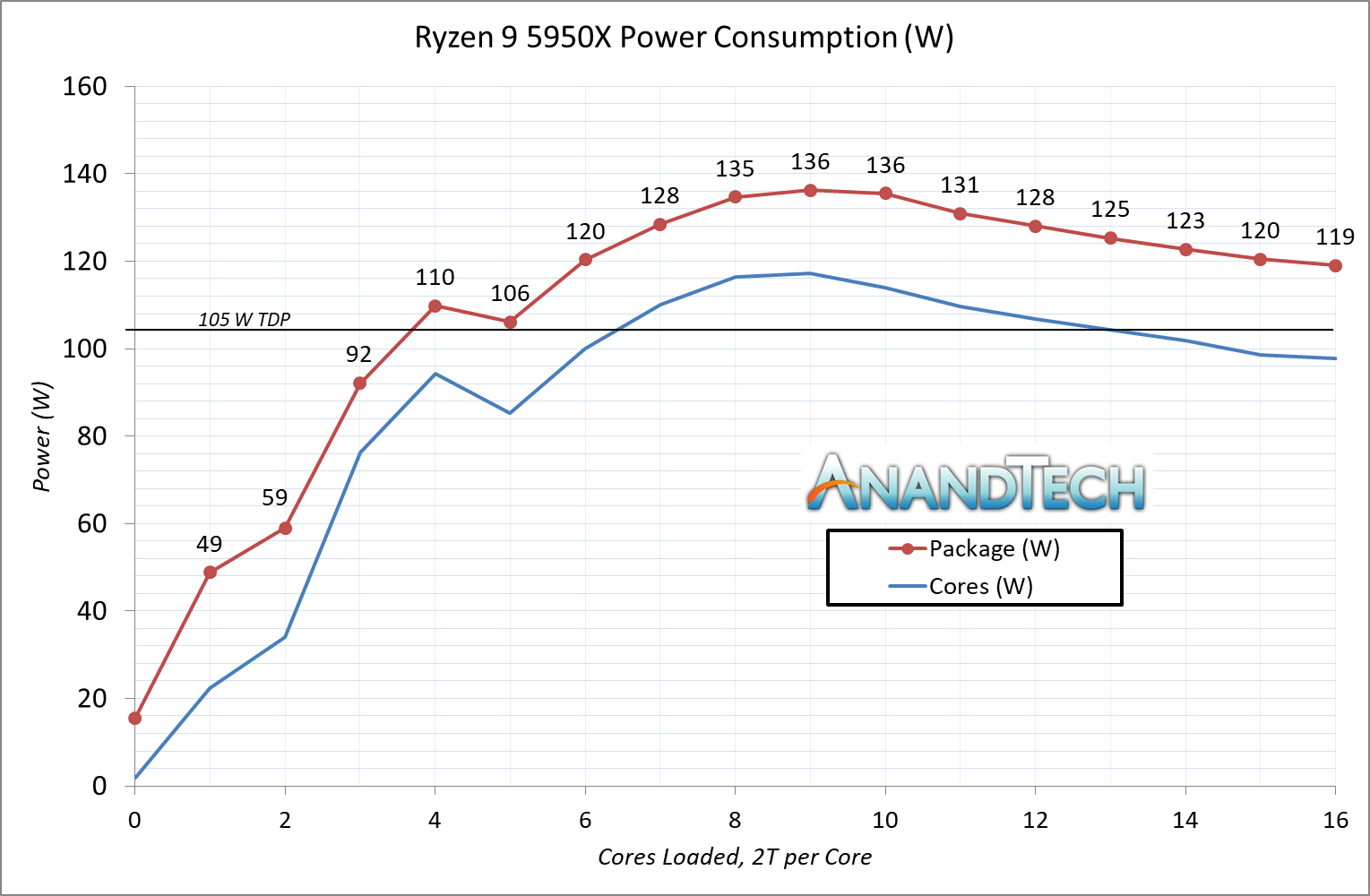
There are two significant features of this graph.
First is the hump, and a slow decrease in total package power consumption after 8-10 core loading. We saw this when we first tested the previous generation 3950X, and is indicative of how the processor has increased current density as it loads up the cores, and as a result there’s a balance between the frequency it can give, delivering the power, and applying the voltage in a consistent way. We’re seeing the difference between the two values also increasing slightly, as more data is transferred over those off-chiplet communications. We see this effect on the 5900X as well, perhaps indicating this is a feature of the dual chiplet design – we’re not seeing it on the 5800X or 5600X.
The second feature is an odd dip in power moving from 4 to 5 cores loaded. Looking into the data, the frequency of the active cores drops from 4725 to 4675, which isn’t a big drop, however the voltage decreases from 1.38 V to 1.31 V, which seems to be more sizeable drop than other voltage readouts as we scale the core-to-core loading. There’s also a bigger increase in non-core power, up from 16 W to 21 W, which perhaps decreases the power to the cores, reducing the voltage.
This might be an odd quirk of our specific chip, our power test, or it might be motherboard or BIOS specific (or a combination of several factors). We might go back in future on other boards to see if this is consistent.
When we dive into per-core power loading, we get the following:
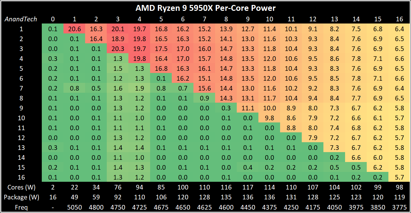
The big chip’s power distribution seems to go up in that 3-4 core loading before coming back down again. But as we load up the second chiplet moving from 8 to 9 core loading, it is worth noting that the second chipset is reporting lower core power, despite showing the same core frequency. AMD is able to supply the two chiplets different amounts of voltage and power, and we might be seeing this play out in real time.
Perhaps very important is that single core power consumption when we are at 5050 MHz of 20.6 W. Going back to our previous generation data, on Zen 2 we were only seeing a peak of 18.3 W, and a slightly higher voltage reported (1.45 V for Zen 2 vs 1.42 V for Zen 3). This means that from the perspective of our two chips, Zen 3 cores scale better in frequency, and even though the power increases as expected, the voltage simultaneously decreases (Note that there can be some silicon variability to also account for some of this.)
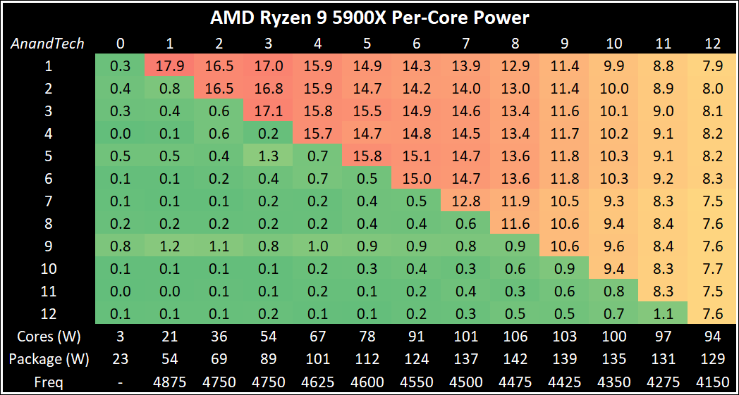
Moving down the stack, the 12-core Ryzen 9 5900X doesn’t show any surprises – we’re seeing the same drop off as we load up the cores, this time as we go beyond eight cores. As this processor uses two chiplets, each with six cores, that second set of six cores seem to be consuming lower power per core as we add in additional load.
Some users might be scratching their heads – why is the second chiplet in both of these chips using less power, and therefore being more efficient? Wouldn’t it be better to use that chiplet as the first chiplet for lower power consumption at low loads? I suspect the answer here is nuanced – this first chipet likely has cores that enable a higher leakage profile, and then could arguably hit the higher frequencies at the expense of the power.
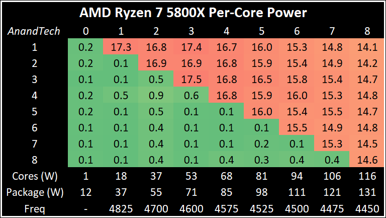
Moving down to a single chiplet but will the full power budget, and there is some power savings by not having the communications of a second chiplet. However, at 8-core load, the 5800X is showing 4450 MHz: the Ryzen 9 processors are showing 4475 MHz and 4500 MHz, indicating that there is still some product differentiation going on with this sort of performance. With this chip we still saw 140 W peak power consumption, however it wasn’t on this benchmark (our peak numbers can come from a number of benchmarks we monitor, not just our power-loading benchmark set).
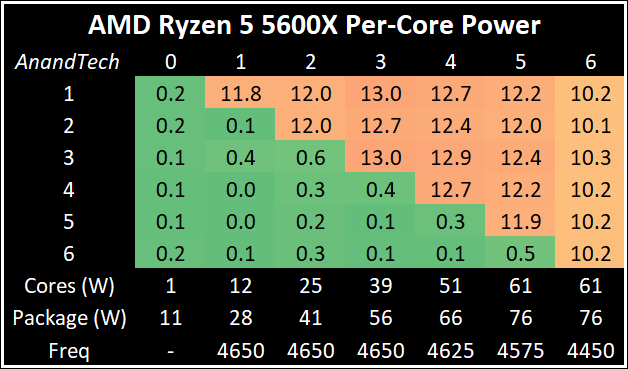
At the 65 W level of the 5600X, as mentioned before, the all-core frequency is 4450 MHz, which is actually 50 MHz behind the 5800X. However this chip is very consistent, still giving up +50 MHz on its peak turbo compared to the on-box number. It also carries this turbo through to at least 3 core loading, and doesn’t lose much to 5 core loading. Users looking for something low power and consistent could be swayed by this chip.
For some specific real-world tests, we’re going to focus solely on the Ryzen 9 5950X. First up is our image-model construction workload, using our Agisoft Photoscan benchmark. This test has a number of different areas that involve single thread, multi-thread, or memory limited algorithms.
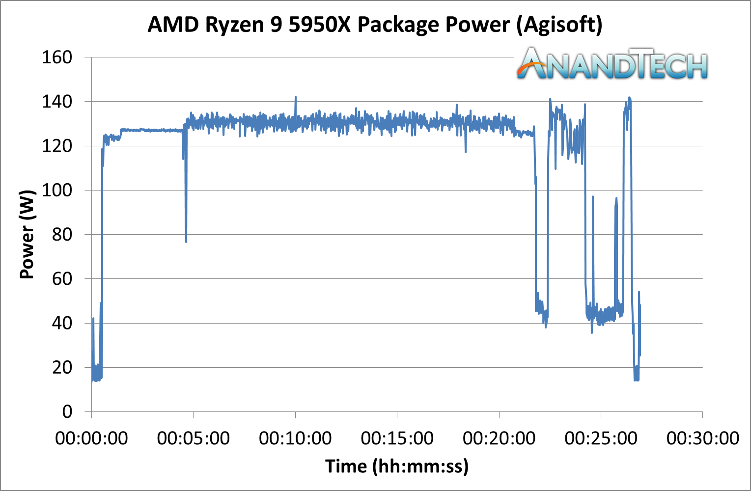
Most of this test sits around the 130 W mark, as the workload has a variable thread count. There are a couple of momentary spikes above 140 W, however everything is well within expected parameters.
The second test is from y-Cruncher, which is our AVX2/AVX512 workload. This also has some memory requirements, which can lead to periodic cycling with systems that have lower memory bandwidth per core options.
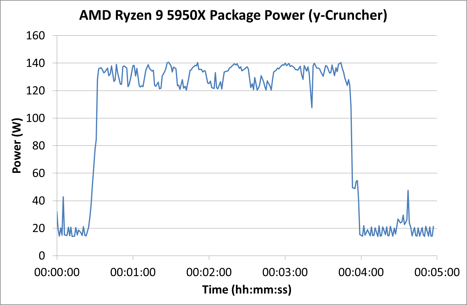
Our y-Cruncher test often shows one of two patterns – either a flat line for power-limited processors, or this zig-zag as the test is loaded and also uses a good portion of memory transfers for the calculation. Usually it is the latter which showcases when we’re getting the most out of the processor, and we get this here.
Compared to other processors, for peak power, we report the highest loaded value observed from any of our benchmark tests.
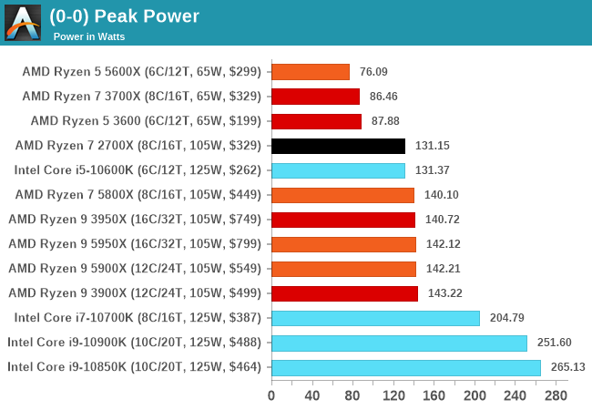
Due to AMD’s PPT implementation, we’re getting very consistent peak power results between multiple generations of AMD processors. Because OEMs play around with Intel’s turbo implementation, essentially to an unlimited peak turbo power, this is why we see full-loaded values well above 200 W. While Intel stays on its most optimized 14nm process and AMD leverages TSMC’s leading 7nm, along with multiple generations of DTCO, AMD will have that efficiency lead.


339 Comments
View All Comments
TheinsanegamerN - Tuesday, November 10, 2020 - link
However AMD's boost algorithim is very temperature sensitive. Those coolers may work fine, but if they get to the 70C range you're losing max performance to higher temperatures.Andrew LB - Sunday, December 13, 2020 - link
Blah blah....Ryzen 5800x @ 3.6-4.7ghz : 219w and 82'c.
Ryzen 5800x @ 4.7ghz locked: 231w and 88'c.
Fractal Celsius+ S28 Prisma 280mm AIO CPU cooler at full fan and pump speed
https://www.kitguru.net/components/cpu/luke-hill/a...
If you actually set your voltages on Intel chips they stay cool. My i7-10700k @ 5.0ghz all-core locked never goes above 70'c.
Count Rushmore - Friday, November 6, 2020 - link
It took 3 days... finally the article load-up.AT seriously need to upgrade their server (or I need to stop using IE6).
name99 - Friday, November 6, 2020 - link
"AMD wouldn’t exactly detail what this means but we suspect that this could allude to now two branch predictions per cycle instead of just one"So imagine you have wide OoO CPU. How do you design fetch? The current state of the art (and presumably AMD have aspects of this, though perhaps not the *entire* package) goes as follows:
Instructions come as runs of sequential instructions separated by branches. At a branch you may HAVE to fetch instructions from a new address (think call, goto, return) or you may perhaps continue to the next address (think non-taken branch).
So an intermediate complexity fetch engine will bring in blobs of instructions, up to (say 6 or 8) with the run of instructions terminating at
- I've scooped up N or
- I've hit a branch or
- I've hit the end of a cache line.
Basically every cycle should consist of pulling in the longest run of instructions possible subject to the above rules.
The way really advanced fetch works is totally decoupled from the rest of the CPU. Every cycle the fetch engine predicts the next fetch address (from some hierarchy of : check the link stack, check the BTB, increment the PC), and fetches as much as possible from that address. These are stuck in a queue connected to decode, and ideally that queue would never run dry.
BUT: on average there is about a branch every 6 instructions.
Now supposed you want to sustain, let's say, 8-wide. That means that you might set N at 8, but most of the time you'll fetch 6 or so instructions because you'll bail out based on hitting a branch before you have a full 8 instructions in your scoop. So you're mostly unable to go beyond an IPC of 6, even if *everything* else is ideal.
BUT most branches are conditional. And good enough half of those are not taken. This means that if you can generate TWO branch predictions per cycle then much of the time the first branch will not be taken, can be ignored, and fetch can continue in a straight line past it. Big win! Half the time you can pull in only 6 instructions, but the other half you could pull in maybe 12 instructions. Basically, if you want to sustain 8 wide, you'd probably want to pull in at least 10 or 12 instructions under best case conditions, to help fill up the queue for the cases where you pull in less than 8 instructions (first branch is taken, or you reach the end of the cache line).
Now there are some technicalities here.
One is "how does fetch know where the branches are, to know when to stop fetching". This is usually done via pre-decode bits living in the I-cache, and set by a kinda decode when the line is first pulled into the I-cache. (I think x86 also does this, but I have no idea how. It's obviously much easier for a sane ISA like ARM, POWER, even z.)
Second, and more interesting, is that you're actually performing two DIFFERENT TYPES of prediction, which makes it somewhat easier from a bandwidth point of view. The prediction on the first branch is purely "taken/not taken", and all you care about is "not taken"; the prediction on the second branch is more sophisticated because if you predict taken you also have to predict the target, which means dealing BTB or link stack.
But you don't have to predict TWO DIFFERENT "next fetch addresses" per cycle, which makes it somewhat easier.
Note also that any CPU that uses two level branch prediction is, I think, already doing two branch prediction per cycle, even if it doesn't look like it. Think about it: how do you USE a large (but slow) second level pool of branch prediction information?
You run the async fetch engine primarily from the first level; and this gives a constant stream of "runs of instructions, separated by branches" with zero delay cycles between runs. Great, zero cycle branches, we all want that. BUT for the predictors to generate a new result in a single cycle they can't be too large.
So you also run a separate engine, delayed a cycle or two, based on the larger pool of second level branch data, checking the predictions of the async engine. If there's a disagreement you flush whatever was fetched past that point (which hopefully is still just in the fetch queue...) and resteer. This will give you a one (or three or four) cycle bubble in the fetch stream, which is not ideal, but
- it doesn't happen that often
- it's a lot better catching a bad prediction very early in fetch, rather than much later in execution
- hopefully the fetch queue is full enough, and filled fast enough, that perhaps it's not even drained by the time decode has walked along it to the point at which the re-steer occurred...
This second (checking) branch prediction doesn't ever get mentioned, but it is there behind the scenes, even when the CPU is ostensibly doing only a single prediction per cycle.
There are other crazy things that happen in modern fetch engines (which are basically in themselves as complicated as a whole CPU from 20 years ago).
One interesting idea is to use the same data that is informing the async fetch engine to inform prefetch. The idea is that you now have essentially two fetch engines running. One is as I described above; the second ONLY cares about the stream of TAKEN branches, and follows that stream as rapidly as possible, ensuring that each line referenced by this stream is being pulled into the I-cache. (You will recognize this as something like a very specialized form of run-ahead.)
In principle this should be perfect -- the I prefetcher and branch-prediction are both trying to solve the *exact* same problem, so pooling their resources should be optimal! In practice, so far this hasn't yet been perfected; the best simulations using this idea are a very few percent behind the best simulations using a different I prefetch technology. But IMHO this is mostly a consequence of this being a fairly new idea that has so far been explored mainly by using pre-existing branch predictors, rather than designing a branch predictor store that's optimal for both tasks.
The main difference is that what matters for prefetching is "far future" branches, branches somewhat beyond where I am now, so that there's plenty of time to pull in the line all the way from RAM. And existing branch predictors have had no incentive to hold onto that sort of far future prediction state. HOWEVER
A second interesting idea is what IBM has been doing for two or three years now. They store branch prediction in what they call an L2 storage but, to avoid things, I'll cal a cold cache. This is stale/far future branch prediction data that is unused for a while but, on triggering events, that cold cache data will be swapped into the branch prediction storage so that the branch predictors are ready to go for the new context in which they find themselves.
I don't believe IBM use this to drive their I-prefetcher, but obviously it is a great solution to the problem I described above and I suspect this will be where all the performance CPUs eventually find themselves over the next few years. (Apple and IBM probably first, because Apple is Apple, and IBM has the hard part of the solution already in place; then ARM because they's smart and trying hard; then AMD because they're also smart but their technology cycles are slower than ARM; and final Intel because, well, they're Intel and have been running on fumes for a few years now.)
(Note of course this only solves I-prefetch, which is nice and important; but D-prefetch remains as a difficult and different problem.)
name99 - Friday, November 6, 2020 - link
Oh, one more thing. I referred to "width" of the CPU above. This becomes an ever vaguer term every year. The basic points are two:- when OoO started, it seemed reasonable to scale every step of the pipeline together. Make the CPU 4-wide. So it can fetch up to 4 instructions/cycle. decode up to 4, issue up to 4, retire up to 4. BUT if you do this you're losing performance every step of the way. Every cycle that fetches only 3 instructions can never make that up; likewise every cycle that only issues 3 instructions.
- so once you have enough transistors available for better designs, you need to ask yourself what's the RATE-LIMITING step? For x86 that's probably in fetch and decode, but let's consider sane ISAs like ARM. There the rate limiting step is probably register rename. So lets assume your max rename bandwidth is 6 instructions/cycle. You actually want to run the rest of your machinery at something like 7 or 8 wide because (by definition) you CAN do so (they are not rate limiting, so they can be grown). And by running them wider you can ensure that the inevitable hiccups along the way are mostly hidden by queues, and your rename machinery is running at full speed, 6-wide each and every cycle, rather than frequently running at 5 or 4 wide because of some unfortunate glitch upstream.
Spunjji - Monday, November 9, 2020 - link
These were interesting posts. Thank you!GeoffreyA - Monday, November 9, 2020 - link
Yes, excellent posts. Thanks.Touching on width, I was expecting Zen 3 to add another decoder and take it up to 5-wide decode (like Skylake onwards). Zen 3's keeping it at 4 makes good sense though, considering their constraint of not raising power. Another decoder might have raised IPC but would have likely picked up power quite a bit.
ignizkrizalid - Saturday, November 7, 2020 - link
Rip Intel no matter how hard you try squeezing Intel sometimes on top within your graphics! stupid site bias and unreliable if this site was to be truth why not do a live video comparison side by side using 3600 or 4000Mhz ram so we can see the actual numbers and be 100% assured the graphic table is not manipulated in any way, yea I know you will never do it! personally I don't trust these "reviews" that can be manipulated as desired, I respect live video comparison with nothing to hide to the public. Rip Intel Rip Intel.Spunjji - Monday, November 9, 2020 - link
I... don't think this makes an awful lots of sense, tbh.MDD1963 - Saturday, November 7, 2020 - link
It would be interesting to also see the various results of the 10900K the way most people actually run them on Z490 boards, i.e, with higher RAM clocks, MCE enabled, etc...; do the equivalent tuning with 5000 series, I'm sure they will run with faster than DDR4-3200 MHz. plus perhaps a small all-core overclock.