A Broadwell Retrospective Review in 2020: Is eDRAM Still Worth It?
by Dr. Ian Cutress on November 2, 2020 11:00 AM ESTBroadwell with eDRAM: Still Has Gaming Legs
As we crossover into the 2020s era, we now have more memory bandwidth from DRAM than a processor in 2015. Intel's Broadwell processors were advertised as having 128 megabytes of 'eDRAM', which enabled 50 GiB/s of bidirectional bandwidth at a lower latency of main memory, which ran only at 25.6 GiB/s. Modern processors have access to DDR4-3200, which is 51.2 GiB/s, and future processors are looking at 65 GiB/s or higher.
At this time, it is perhaps poignant to take a step back and understand the beauty of having 128 MiB of dedicated silicon for a singular task.
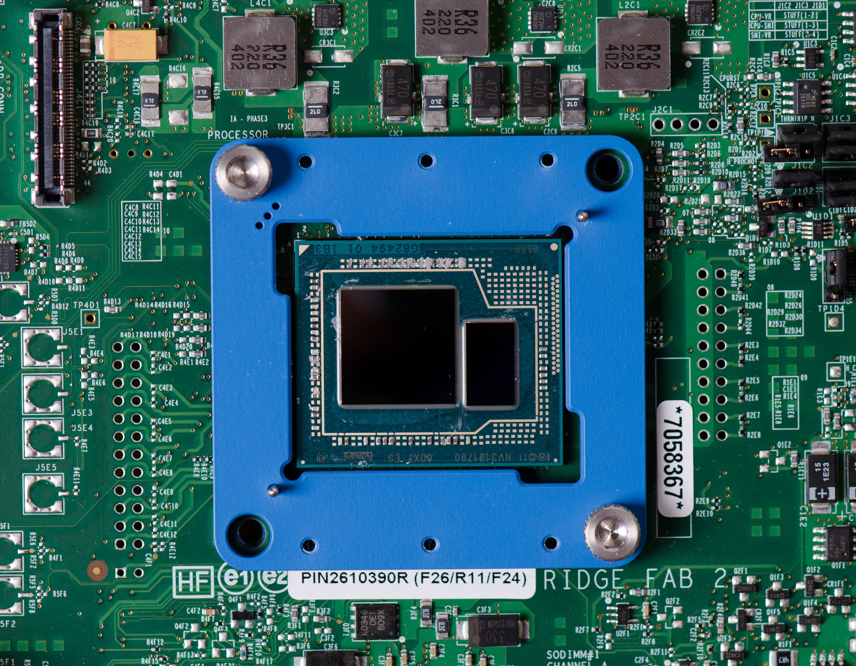
Intel’s eDRAM enabled Broadwell processors accelerated a significant number of memory bandwidth and memory latency workloads, in particular gaming. What eDRAM has enabled in our testing, even if we bypass the now antiquated CPU performance, is surprisingly good gaming performance. Most of our CPU gaming tests are designed to enable a CPU-limited scenario, which is exactly where Broadwell can play best. Our final CPU gaming test is a 1080p Max scenario where the CPU matters less, but there still appears to be good benefits from having an on-die DRAM and that much lower latency all the way out to 128 MiB.
There have always been questions around exactly what 128 MiB of eDRAM cost Intel to produce and supply to a generation of processors. At launch, Intel priced the eDRAM versions of 14 nm Broadwell processors as +$60 above the non-eDRAM versions of 22 nm Haswell equivalents. There are arguments to say that it cost Intel directly somewhere south of $10 per processor to build and enable, but Intel couldn’t charge that low, based on market segmentation. Remember, that eDRAM was built on a mature 22 nm SoC process at the time.
As we move into an era where AMD is showcasing its new ‘double’ 32 MiB L3 cache on Zen 3 as a key part of their improved gaming performance, we already had 128 MiB of gaming acceleration in 2015. It was enabled through a very specific piece of hardware built into the chip. If we could do it in 2015, why can’t we do it in 2020?
What about HBM-enabled eDRAM for 2021?
Fast forward to 2020, and we now have mature 14 nm and 7 nm processes, as well as a cavalcade of packaging and eDRAM opportunities. We might consider that adding 1-2 GiB of eDRAM to a package could be done with high bandwidth connectivity, using either Intel’s embedded multi-die technology or TSMC’s 3DFabric technology.
If we did that today, it could arguably be just as complex as what it was to add 128 MiB back in 2015. We now have extensive EDA and packaging tools to deal with chiplet designs and multi-die environments.
So consider, at a time where high performance consumer processors are in the realm of $300 up to $500-$800, would customers consider paying +$60 more for a modern high-end processor with 2 gigabytes of intermediate L4 cache? It would extend AMD’s idea of high-performance gaming cache well beyond the 32 MiB of Zen 3, or perhaps give Intel a different dynamic to its future processor portfolio.
As we move into more a chiplet enabled environment, some of those chiplets could be an extra cache layer. However, to put some of this into perspective.
- Intel's Broadwell's 128 MiB of eDRAM was built (is still built) on Intel's 22nm IO process and used 77 mm2 of die area.
- AMD's new RX 6000 GPUs use '128 MiB' of 7nm Infinity Cache SRAM. At an estimated 6.4 billion transistors, or 24% of the 26.8 billion transistors and ~510-530mm2 die, this cache requires a substantial amount of die area, even on 7nm.
This would suggest that in order for future products to integrate large amounts of cache or eDRAM, then layered solutions will need to be required. This will require large investment in design and packaging, especially thermal control.
Many thanks to Dylan522p for some minor updates on die size and pointing out that the same 22nm eDRAM chip is still in use today with Apple's 2020 base Macbook Pro 13.


120 Comments
View All Comments
realbabilu - Monday, November 2, 2020 - link
That Larger cache maybe need specified optimized BLAS.Kurosaki - Monday, November 2, 2020 - link
Did you mean BIAS?ballsystemlord - Tuesday, November 3, 2020 - link
BLAS == Basic Linear Algebra System.Kamen Rider Blade - Monday, November 2, 2020 - link
I think there is merit to having Off-Die L4 cache.Imagine the low latency and high bandwidth you can get with shoving some stacks of HBM2 or DDR-5, whichever is more affordable and can better use the bandwidth over whatever link you're providing.
nandnandnand - Monday, November 2, 2020 - link
I'm assuming that Zen 4 will add at least 2-4 GB of L4 cache stacked on the I/O die.ichaya - Monday, November 2, 2020 - link
Waiting for this to happen... have been since TR1.nandnandnand - Monday, November 2, 2020 - link
Throw in an RDNA 3 chiplet (in Ryzen 6950X/6900X/whatever) for iGPU and machine learning, and things will get really interesting.ichaya - Monday, November 2, 2020 - link
Yep.dotjaz - Saturday, November 7, 2020 - link
That's definitely not happening. You are delusional if you think RDNA3 will appear as iGPU first.At best we can hope the next I/O die to intergrate full VCN/DCN with a few RDNA2 CUs.
dotjaz - Saturday, November 7, 2020 - link
Also doubly delusional if think think RDNA3 is any good for ML. CDNA2 is designed for that.Adding powerful iGPU to Ryzen 9 servers literally no purpose. Nobody will be satisfied with that tiny performance. Guaranteed recipe for instant failure.
The only iGPU that would make sense is a mini iGPU in I/O die for desktop/video decoding OR iGPU coupled with low end CPU for an complete entry level gaming SOC aka APU. Chiplet design almost makes no sense for APU as long as GloFo is in play.