The Intel Xe-LP GPU Architecture Deep Dive: Building Up The Next Generation
by Ryan Smith on August 13, 2020 9:00 AM EST- Posted in
- GPUs
- Intel
- Tiger Lake
- Xe
- Xe-LP
- DG1
- Intel Arch Day 2020
- SG1
Xe-LP By the Slice: 50% Larger With 96 EUs
Instead of focusing on high-level graphics features, the bulk of Intel’s attention has instead gone to the low-level architectural details of their GPUs. Xe-LP is the building block to many more Xe GPUs to come, so this is an area where Intel needed to get things right – both in design and power efficiency – in order to have a stable foundation for building future products.
And to be sure, that foundational analogy extents within Intel’s earlier GPU designs as well. While Xe is new branding and the start of something much bigger for Intel, it isn’t a clean sheet design of Intel’s GPUs. Rather it’s a focused evolution of Gen11, updating and replacing those bits that need to be altered for scalability or efficiency reasons. Consequently, there’s a good deal that is held over from Gen11, and the basic organizational structure of Intel’s GPUs remains the same.
| Intel GPU Specification Comparison | ||||||
| Xe-LP (Tiger Lake) |
Xe-HPG | Gen11 (Ice Lake) |
Gen9.5 (Kaby Lake) |
|||
| ALUs | 768 | Many | 512 | 192 | ||
| Texture Units | 48 | Lots | 32 | 12 | ||
| ROPs | 24 | Yes Please | 16 | 8 | ||
| Peak Clock | 1600MHz+ | Better Than Xe-LP | 1100MHz | 1150MHz | ||
| Throughput (FP32) | 2.46 TFLOPs | All of the FLOPs | 1.13 TFLOPs | 0.44 TFLOPs | ||
| Memory Clock | LPDDR4X-4266 | GDDR6 | LPDDR4X-3733 | DDR4-2133 | ||
| Memory Bus Width | 128-bit (IMC) |
Sizable | 128-bit (IMC) |
128-bit (IMC) |
||
| Geometry Rate (Prim/Clock) |
2 | 2x # of Slices | 1 | 1 | ||
| Manufacturing Process | Intel 10nm SuperFin | "External" | Intel 10nm | Intel 14nm+ | ||
| Architecture | Xe-LP | Xe-HPG | Gen11 | Gen9.5 | ||
| GPU | Tiger Lake Integrated |
Xe-HPG | Ice Lake Integrated | Kaby Lake Integrated | ||
| Launch Date | 09/2020 | 2021 | 09/2019 | 01//2017 | ||
As always then, this means we’ll start with the Xe-LP Slice and Intel’s overall GPU design goals. Intel’s largest common building block, the company’s GPUs are organized into one or more slices, with a single slice containing a full copy of the core functional blocks needed for compute and rendering. This includes the geometry and raster frontend, thread dispatch hardware, the EUs themselves, texture units, and the ROP pixel backends.
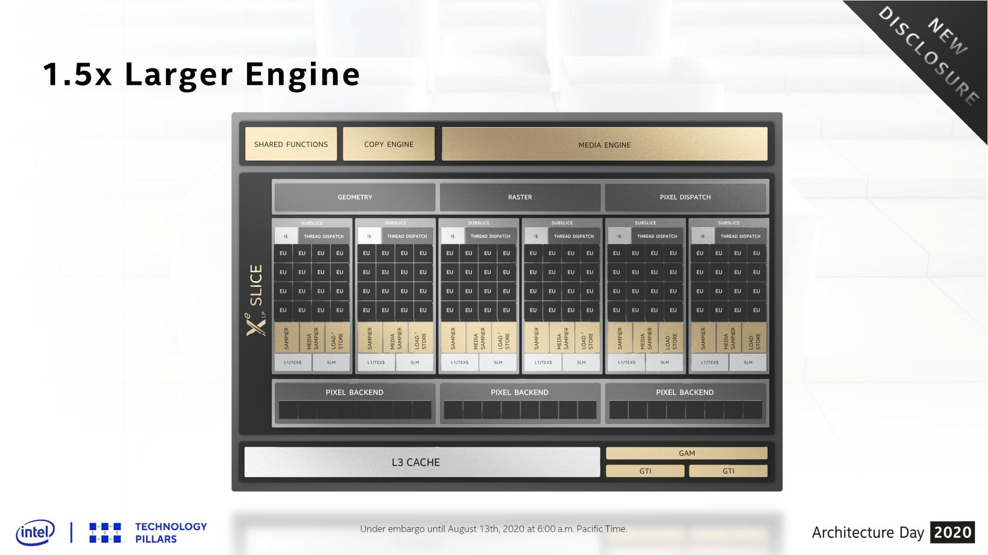
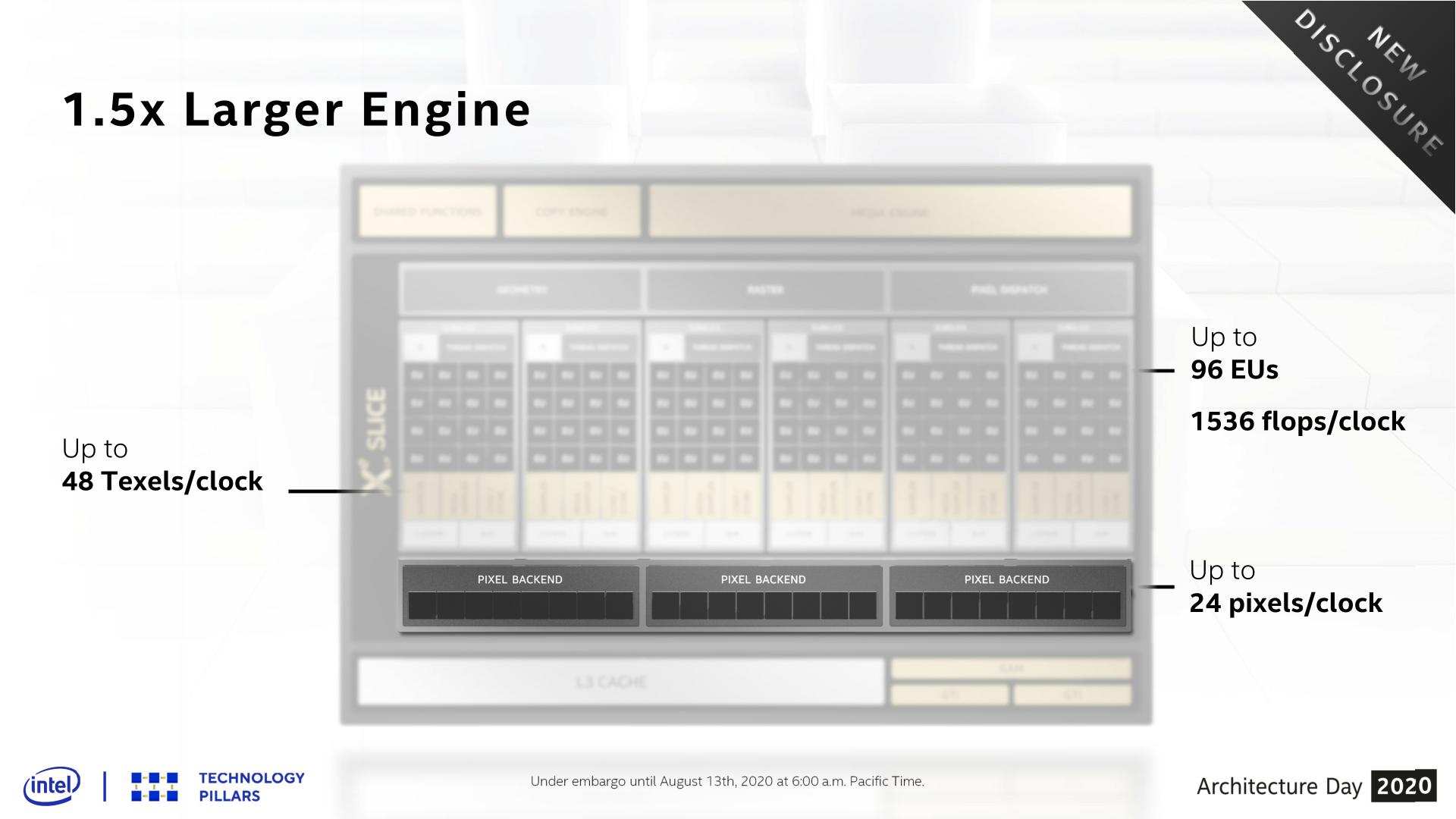
With Xe-LP, Intel has expanded almost everything about a slice by 50%. Which means that versus Intel’s Gen11 iGPUs, which happened to top out a single slice, there’s 50% more execution hardware to play with for most aspects of the GPU. This includes 50% more EUs – bringing the total there to 96 EUs – as well as 50% more texture units and 50% more ROPs, for a total rate of 48 texels/clock and 24 pixels/clock respectively.
The only part of the slice that hasn’t been explicitly scaled up by such a factor is the frontend. There is still a single geometry/rasterizer/pixel dispatch frontend feeding the rest of the slice, and as Intel hasn’t disclosed any changes in geometry throughput, I am assuming here that Intel is still only dispatching 1 primative-per-clock-per-slice. So any improvement there will have to come from clockspeeds.
Update: Intel has since shot me a note stating that they have in fact upgraded their geometry front-end, so this is not the same 1 triangle/clock hardware as on earlier Intel GPUs. Xe-LP's geometry frontend can now spit out two backface culled triangles per clock, doubling Intel's peak geometry performance on top of Xe-LP's clockspeed improvements.
Performance aside, this is a big step up for Intel's GPU design, as scaling a GPU above 1 triangle/clock requires a significant rework of its geometry processing capabilities. By definition, a GPU with a 2+ triangle rate needs to be able to handle multiple triangles at once – essentially converting a serial process to a parallel process, with all the added complexity that entails. Furthermore, since the geometry engine is part of the Slice, that means larger Xe-LP designs (and Xe-HPG) will be able to scale up their geometry frontends by even more, as the geometry engine would get replicated with every slice. This is a notable distinction from earlier multi-Slice designs like Gen9 GT4e, where the geometry engine was part of the "unslice" and therefore was a fixed frontend for the entire GPU.
Moving on, let's talk about clockspeeds. As was the case with Intel’s Willow Cove CPU cores, the company is banking hard on the energy efficiency and clockspeed improvements of their new 10nm SuperFin process to allow them to boost GPU clockspeeds to meet their performance goals. As we previously discussed, Intel is looking to double GPU performance versus Gen11 here, and with 50% more execution hardware only covering at most half of that need, much of the rest of the increase will come from higher clockspeeds. Intel’s Ice Lake parts, for reference, topped out at 1.1GHz, so it wouldn’t be too surprising to see Tiger Lake and DG1 to run at 1.6GHz or better, given Intel’s performance projections.
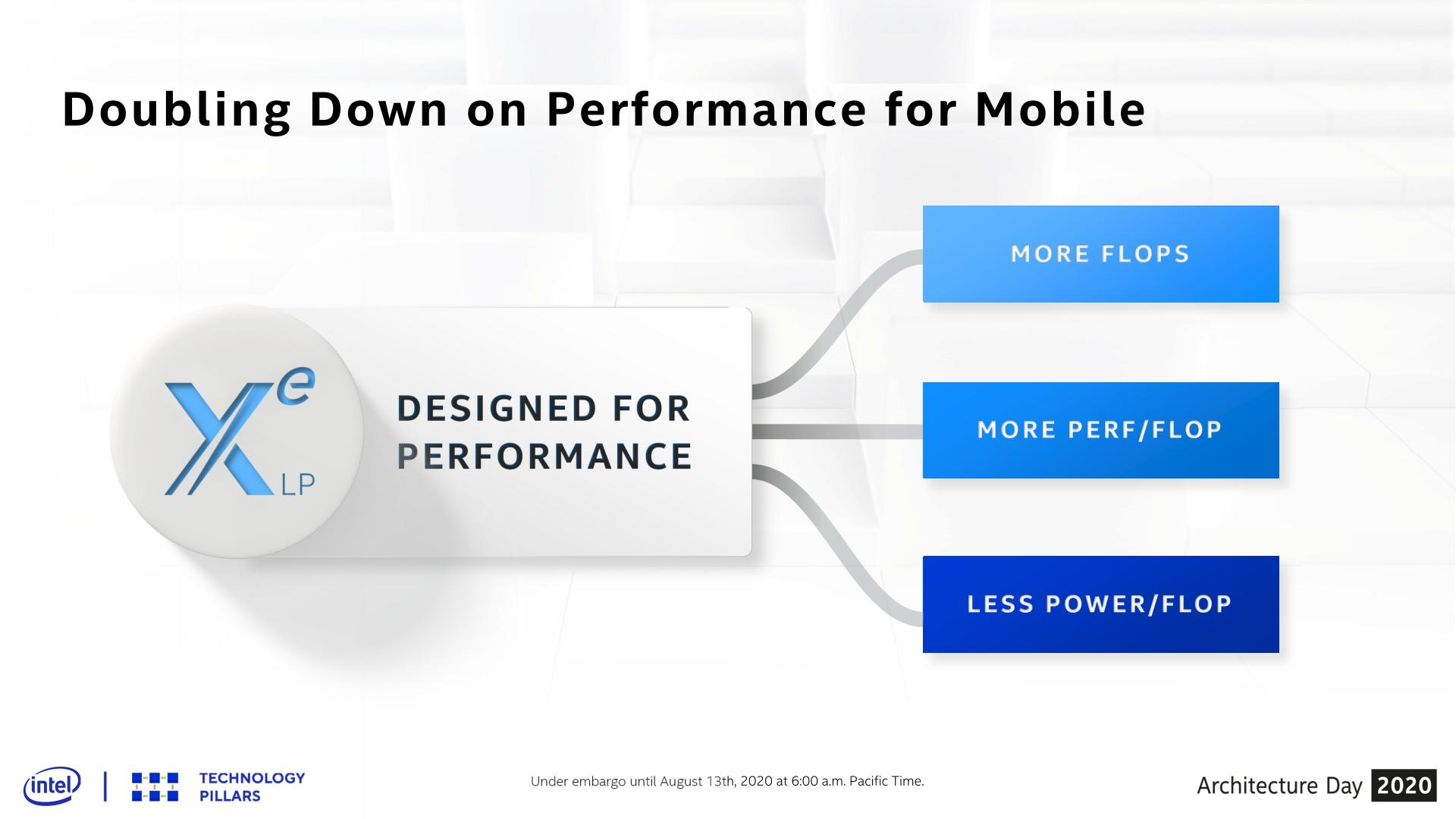
Rounding out Intel’s plan to boost GPU performance then comes from the third pillar of Xe-LP’s design, which is improving efficiency. While adding EUs adds FLOPs, and improving energy efficiency allows Intel to clock the chip higher to add even more FLOPs, adding FLOPs alone isn’t enough. Work must also go into improving the effective throughput of an architecture, to covert more of those theoretical FLOPs into real-world work.
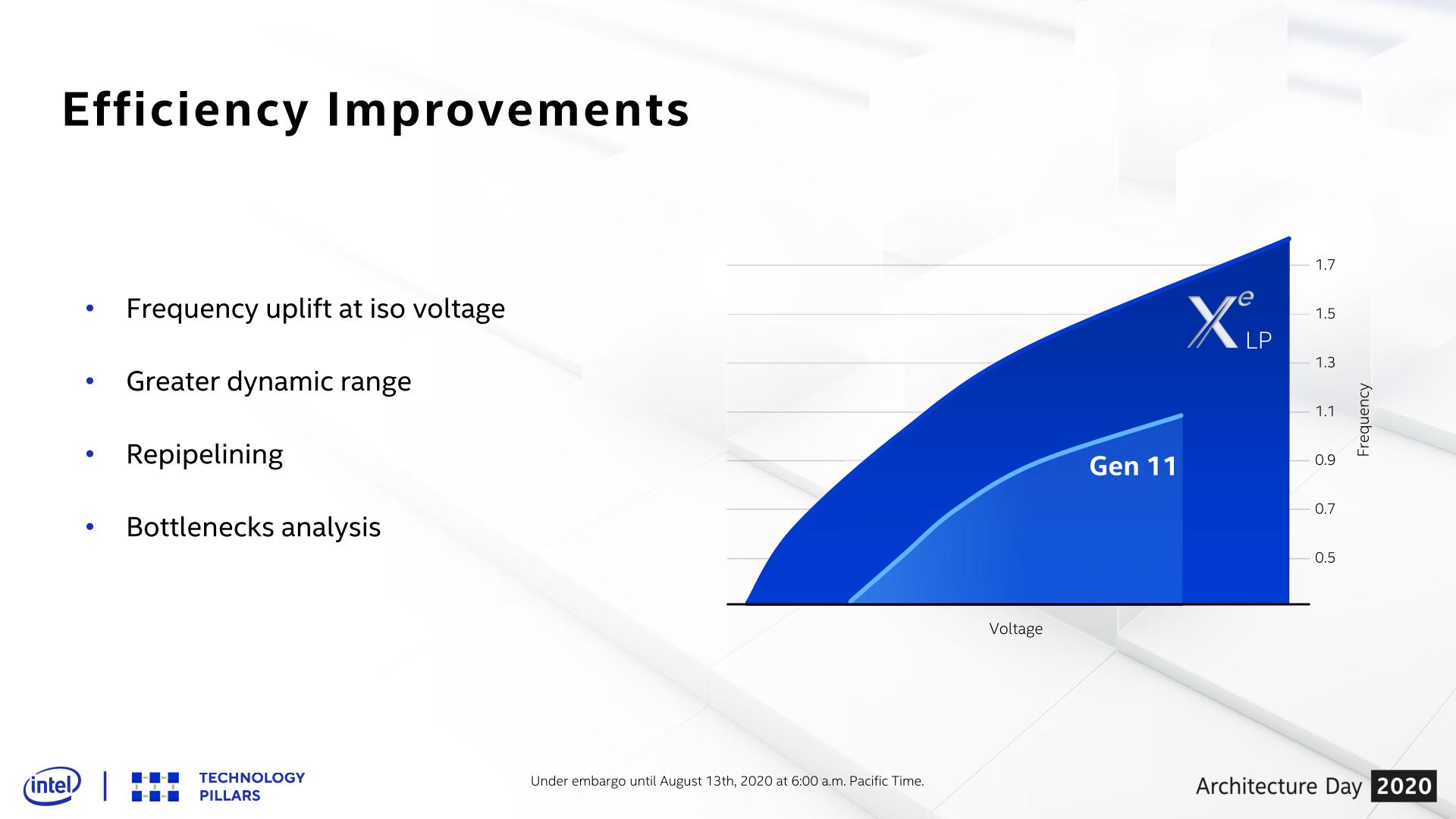
And this is where Intel’s secret sauce comes in, and not as much from Intel’s technical marketing department comes out. There are some notable low-level EU changes that we’ll get to in a moment, but these are more about driving the aforementioned power efficiency changes. Instead, the throughput efficiency changes are more opaque. Here Intel merely tells us that they’ve used workload analysis to identify and remove multiple small bottlenecks throughout the GPU to improve graphics and compute throughput efficiency.
Intel’s L1 cache changes likely also play a part here, though the company isn’t going too much into those changes at this time. None the less, we’ll catch up on the subject in a bit when looking at the overall memory system.
Subslice Reorganization
One further consequence of widening the overall slice is that Intel has reorganized the subslice within the larger slice. Analogous in a few ways to NVIDIA’s SMs, a subslice is a smaller building block within the GPU, focused on compute and shading in all forms, as well as texturing. For Intel’s Gen11 GPUs, the company organized the GPUs into 8 subslices, each containing 8 EUs. But with Xe-LP, each subslice has been bulked up, and the number of overall subslices has been reduced.
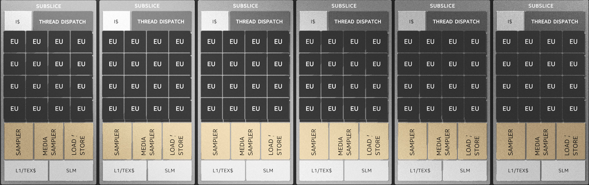
A full slice on Xe-LP is now 6 subslices. Each Xe-LP subslice, in turn, has seen many of its attributes doubled. The number of EUs in a subslice is doubled to 16 per, and the throughput of a subslice’s texture sampler has been bumped up from 4 texels/clock to 8 texels/clock. Each subslice also gets an L1 data/texture cache, which is 64KB and can be dynamically allocated between L1 data and texture storage. This cache would seem to replace Gen11’s poorly documented L2 cache, which occupied a similar role in the hierarchy.
These subslice changes, in turn, go hand-in-hand with some of the changes Intel made to the EUs, which we’ll cover on the next page. With EUs losing a little bit of their independence and getting paired off, this keeps the number of thread control units per subslice constant at 8. It’s likely to also help Intel’s scalability towards future solutions, as they have fewer subslices to wrangle and manage overall.
One consequence of this change means that Intel’s iGPU scalability steps will also be a bit different. Whereas Ice Lake shipped with 64 EUs (8 subslices), 48 EUs (6 subslices), or 32 EUs (4 subslices) enabled, depending on the SKU, Tiger Lake’s granularity is now one-sixth of a slice. So that means half of a GPU is now 48 EUs (3 subslices), a full GPU is 96 EUs (6 subslices), and Intel will have to decide if and how it wants to ship SKUs in the middle with 80 or 64 EUs enabled. As Intel isn’t providing production information today, we can only speculate, but it would be a pretty huge drop in performance if the next tier down after a fully-enabled Xe-LP iGPU was a 64 EU configuration, shedding 33% of its potential performance along the way.


33 Comments
View All Comments
mode_13h - Thursday, August 13, 2020 - link
I can't speak to Direct 3D, but OpenGL talks about work group invocations. I don't believe "threads" is mentioned anywhere in the API.Dolda2000 - Thursday, August 13, 2020 - link
Admittedly I haven't read the whole article yet, but it strikes me how the presentations seems to be comparing the new GPU to the previous GPU, rather than presenting it as a new architecture. Does this confirm that using the "Xe" moniker for this product is just marketing, and that it in fact is an evolution of previous Gen architectures?I mean, I don't mind if that's the case, I just wish they wouldn't overmarket it.
Ryan Smith - Thursday, August 13, 2020 - link
" is an evolution of previous Gen architectures?"It is an evolution of the previous Gen architectures. A major evolution, but an evolution none the less. Not even Intel is going to do a clean sheet design when they have bits and pieces that already work fine.
Dolda2000 - Thursday, August 13, 2020 - link
Certainly, they're not going to create a new clean-slate ALU design just for the sake of it, but it has always been my impression that Xe (at least Xe-HPC) was going to be a more-or-less new architecture. Maybe that has just been my misunderstanding the whole, and Xe-HPC too is going to be fundamentally Gen-based (though I seem to recall that being explicitly denied at some point), but what I was getting at here was that Xe-HPC is going to be the new architecture, and meanwhile this is "merely" an evolution of Gen for which they're just borrowing the product name of their higher-end offering to make it seem like more than what it is.mode_13h - Thursday, August 13, 2020 - link
You should distinguish between the ISA and uArch of the shader cores (EUs) vs. the macro-architecture of the GPU (e.g. buses, memories, caches, fixed-function units, etc.).So, you can have a macro-architecture that's *very* different, even while the ISA is a small evolution and the uArch of the EUs is somewhere in between.
tipoo - Thursday, August 13, 2020 - link
RDNA 1 still has significant GCN bits in it, I'm sure Nvidia does the same a few generations in a row, there's no necessary contention between it being an evolution and it being marked as something substantially new.abufrejoval - Thursday, August 13, 2020 - link
IMHO the overhead of multi GPU rendering with an iGPU and dGPU can't really be offset by the small contribution the iGPU is likely to make to a beefy dGPU.More likely will be dGPU via Thunderbolt 4 and very seamless transitions on docking/undocking and that's good enough.
Too bad that won't work nearly as well with Ryzen notebooks so there again consumer choice goes down the drain somewhat. Not that I believe TB dGPU is a really an attractive market unless prices change dramatically.
mode_13h - Thursday, August 13, 2020 - link
Agreed. I think it would work much better to task the iGPU with other compute tasks that involve less communication bandwidth with the dGPU. Things like physics, AI, audio processing, etc.brucethemoose - Thursday, August 13, 2020 - link
Maybe post processing? Like an Intel version lf ReShade? IIRC the frames have to come back to the IGPU's display block anyway.tipoo - Thursday, August 13, 2020 - link
In this case the IGP would be nearly equivalent to DG1