The Intel Lakefield Deep Dive: Everything To Know About the First x86 Hybrid CPU
by Dr. Ian Cutress on July 2, 2020 9:00 AM ESTHow To Treat a 1+4 Hybrid CPU
At the top of the article, I explained that the reason for using two different types of processor core, one big on performance and the other big on efficiency, was that users could get the best of both worlds depending on if a workload could be run efficiently in the background, or needed the high performance for a user experience interaction. You may have caught onto the fact that I also stated that because Intel is using a 1+4 design, it actually makes more sense for multi-threaded workloads to run on the four Atom cores.
Using a similar power/performance graphs, the effect of having a 1+4 design is quite substantial. On the left is the single core power/performance graphs, but on the right is when we compare 1 Sunny Cove to all 4 Tremont cores working together.
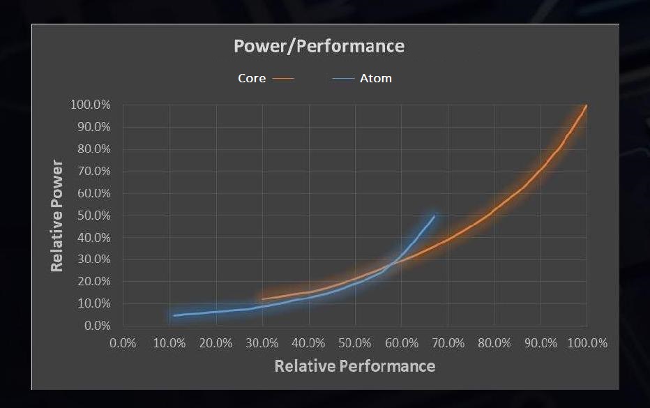
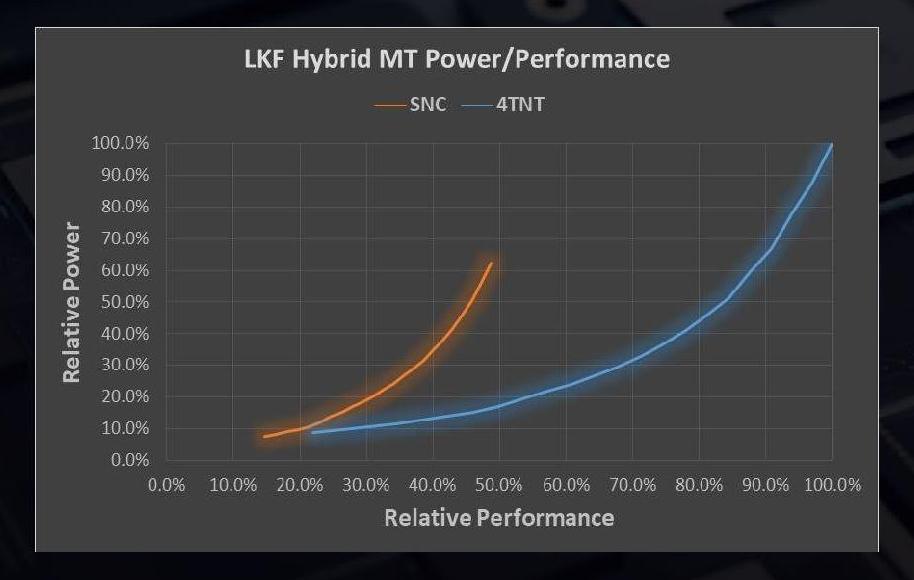
Where the previous graph considered a 1+1 design, which is more relevant in those user experience scenarios listed above, on the right is the 1+4 design for when the user demands a heavier workload that might not be latency critical. Because there are four Atom cores, the blue line multiplies by four in both directions.
Now obviously the real world scenario is somewhere between the two, as it is possible to use only one, two, or three of the smaller cores at any given time. The CPU and the OS is expected to know this, so it can govern when workloads that can be split across multiple cores end up on either the big core or the small core.
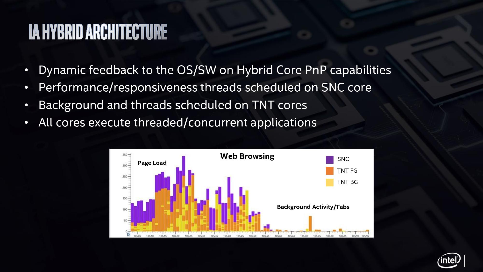
In this graph from Intel, we have three distinct modes on which threads can operate.
- ‘Sunny Cove/SNC’ is for responsiveness and user experience threads,
- ‘Tremont/TNT Foreground’, for user related tasks that require multiple threads that the user is waiting on.
- ‘Tremont/TNT Background’, for non-user related tasks run in efficiency mode
Even though the example here is web browsing, it might be best to consider something a bit beefier, like video encoding.
If we run video encoding, because it is a user related task that requires multiple threads, it will run on the four Tremont cores (TNT FG). Anything that Windows wants to do alongside that gets scheduled as TNT BG. If we then open up the start menu, because that is a responsiveness task, that gets scheduled on the SNC core.
Is 1+4 the Correct Configuration?
Intel here has implemented a 1+4 core design, however in the smartphone space, things are seen a little differently. The most popular configuration, by far, is a 4+4 design, simply because a lot of smartphone code is written to take advantage of multiple foreground or multiple background threads. There are a number of cost-down designs that reduce die area and power by going for a 2+4 implementation. Everyone seems adamant that 4 is a good number for the smaller cores, partly because they are small and cheap to add, but because Arm’s quad-core implementation is a base unit for its IP.
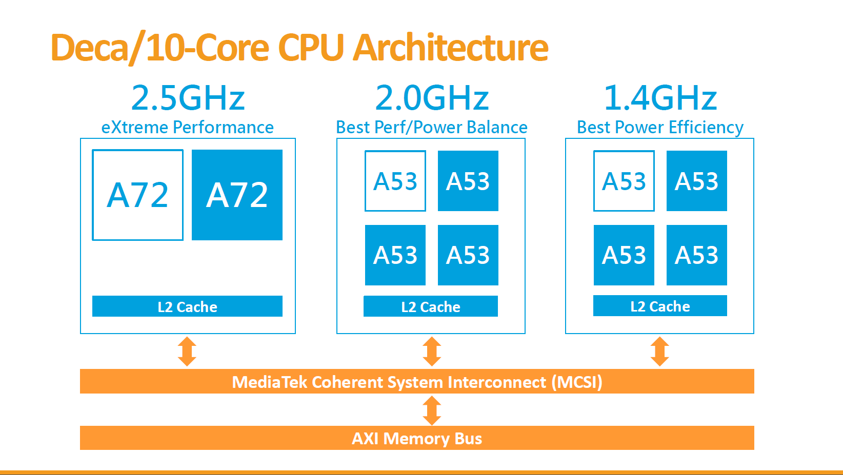
The smartphone space in recent quarters has also evolved from a two tier system of cores. In some of the more leading edge designs, we now have three types of core: a big, a middle, and a small. Because of the tendency to stay with eight core designs, we now get 1+3+4 or 2+2+4 designs, powered by complex schedulers that manage where to put the threads for the best user experience, the best battery life, or somewhere in the middle. Mediatek has been famously dabbling in 10 core designs, going for a 2+4+4 approach.
One thing missing from all of these implementations is an SoC with one big core and four small cores. Smartphone vendors don’t seem to be interested in 1+4 silicon, and yet Intel has decided on it for Lakefield. This is borne out of decisions made on both sides.
From the smartphone perspective, when hybrid designs came about, the big cores just weren’t powerful enough on their own. In order to offer something more than simply basic, at least two cores were needed, but because of how Arm architected the big and little designs, it almost became standard to look into 4+4 implementations of big and small cores. It was only until this configuration was popularized over a couple of years, and Arm big cores got more powerful, that chip designs started looking at 2+4, or 1+3+4 designs.
On Intel’s side of the fence, the biggest problem it has is the size of the Sunny Cove core. By comparison, it’s really, really big. Because the graphics core is the same as Ice Lake and reuses its design, there simply isn’t enough room within the 82 mm2 compute die to add another core. Not only that, but there is a question of power. Sunny Cove wasn’t built for sub-1W operation, even in the Tremont design. We see big smartphone silicon pulling 4-5W when all eight cores are active – there is no way, based on our understanding of Intel’s designs, that we could see four (or even two) Sunny Cove cores being in the optimal performance per watt range while being that low. Intel’s Lakefield graphics, with 64 EUs, is running at only 500 MHz – a lot lower than the Ice Lake designs. Even if Intel moved that down to a 32 EU design to make space for another Sunny Cove core, I reckon that it would eat the power budget for breakfast and then some.
Intel has made the 1+4 design to act as a 0+4 design that sometimes has access to a higher performance mode. Whereas smartphone chips are designed for all eight cores to power on for sustained periods, Lakefield is built only for 0+4 sustained workloads. And that might ultimately be its downfall. This leads onto a deep discussion about Lakefield’s performance, and what we should expect from it.


221 Comments
View All Comments
ichaya - Sunday, July 5, 2020 - link
The chart shows <10% power for <30% perf, and <20% power for <50% perf. That seems like 2-3x perf/watt difference as well. The A13 has a total of 28MB of cache shared between the CPU+GPU, where as this seems to have 6MB for the 4+1 CPU cores sans L1 caches.I'd love to see an Anandtech article on how Apple's large caches help with the code density differences between x86-64/ARM and with lower clock speeds, power consumption.
Wilco1 - Sunday, July 5, 2020 - link
The code density of AArch64 is significantly better than x86_64, so even at same cache sizes Arm has an advantage.ichaya - Wednesday, July 8, 2020 - link
Source? Everything I've read says x86-64 still has a diminishing but slight advantage in code density. If anything, lower clock speeds are helping Apple by avoiding memory pressure issues at higher clock speeds. I highly doubt AArch64 could perform the same as x86-64 with equal caches at any clock speed. uArch differences could outweigh these differences, but I've seen evidence of this given how large Apple's caches have been.ichaya - Wednesday, July 8, 2020 - link
* I've seen no evidence of this given how large Apple's caches have been.Correcting the last sentence in post above.
Wilco1 - Wednesday, July 8, 2020 - link
No, x86 has never had good code density, 32-bit x86 is terrible compared to Thumb-2. x86_64 has worse code density than 32-bit x86, and it gets really bad if you use SIMD instructions.Try building a large binary on both systems using the same compiler and compare the .text sizes. For example I use all of SPEC2017 built with identical GCC version and options. AArch64 code is generally 10-15% smaller.
Many AArch64 cores already have higher IPC - yes that absolutely means they are faster than x86 cores at the same clock frequency using similar sized caches.
This https://images.anandtech.com/graphs/graph15578/115... shows Neoverse N1 has ~28% higher IPC than EPYC 7571 and ~21% higher IPC than Xeon Platinum 8259 on SPECINT2017. While Naples has 2x8MB LLC on each chiplet, the Xeon has 36MBytes, more than the 32MB in Graviton 2 (both also have 1MB L2 per core).
Recent cores like Cortex-A78 and Cortex-X1 are 30-50% faster than Neovere N1. Do the math and see where this is going. 2020 is the year when AArch64 servers outperform the fastest x86 servers, 2021 may be the year when AArch64 CPUs outperform the fastest x86 desktops.
ichaya - Saturday, July 11, 2020 - link
If you compare with -march=x86-64 or with a specific uArch like -march=haswell you'll get comparable code sizes to -march=armv8.4-a. But form the runtime code density differences I've seen, x86-64 still seems to have a slight advantage.From the article you linked the image from (https://www.anandtech.com/show/15578/cloud-clash-a... "If we were to divide the available cache on a per-thread basis, the Graviton2 leads the set at 1.5MB, ahead of the EPYC’s 1.25MB and the Xeon’s 1.05MB." ARM's system-level cache is good idea, as is shared L2 in Apple's A* chips. But cache advantages per thread in Graviton and A* seem to signal it's not the uArch making the difference. Similar cores to Graviton's cores with less cache, do a lot worse. Not being able to clock higher than 2.5Ghz also seems to signal that the uArch/interconnects cannot keep up with memory pressure.
To the extent that die sizes of these chips (Graviton 2 is 7nm, Epyc 7571 and Intel Xeon 8259CL are 14nm) are comparable, it's features like AVX2/SMT that seem to have been replaced with cache in the benchmarks in the article. I'll be looking forward to A* chips to see how they might stack up in Laptops and Desktops, but these are the doubts I still have.
ichaya - Saturday, July 11, 2020 - link
Correct link in post above: https://www.anandtech.com/show/15578/cloud-clash-a...Wilco1 - Saturday, July 11, 2020 - link
Runtime code density? Do you mean accurately counting total bytes fetched from L1I and MOP cache? x86 won't look good because of the inefficiency of byte-aligned instructions, needing 2 extra predecode bits per byte and MOPs being very wide on x86 (64 bits in SandyBridge)... It clearly shows why byte-sized instructions are a bad idea.The graph I posted is for single-threaded performance, so the amount of cache per-thread is not relevant at all. Arm's IPC is higher and thus it is a better micro architecture than Skylake and EPYC 1. IPC is also ~12% better than EPYC 7742 based on https://www.anandtech.com/show/14694/amd-rome-epyc...
In terms of all-core throughput the fastest EPYC 7742 does only ~30% better than Graviton 2 on INTrate2006. That's pretty awful considering it has 8 times the L3 cache (yes eight times!!!), twice the threads, runs at up to 3.4GHz and uses twice the power...
In terms of die size, EPYC 7742 is ~3 times larger in 7nm, so it's extremely area inefficient compared to Graviton 2. So any suggestion that cache is used to make a weak core look better should surely be directed at EPYC?
Graviton 2 is a very conservative design to save cost, hence the low 2.5GHz frequency. Ampere Altra pushes the limits with 80 Neoverse N1 cores at 3.3GHz base (yes that's base, not turbo!). Next year it will have 128 cores, competing with 128 threads in EPYC 3. Guess how that will turn out?
ichaya - Sunday, July 12, 2020 - link
Code density and decoding instructions are separate things. Here's an older paper on code density of a particular program: http://web.eece.maine.edu/~vweaver/papers/iccd09/l...Single threaded workloads are obviously going to do better with a shared system-level and in Apple's case, shared L2 caches. Sharing caches is something that Intel is closer to than AMD. You cannot compare INTrate2006 or any single threaded benchmark running on an ARM where all system-level caches are available for one thread with an Epyc 7742 where only 1 CCX's L3 caches are available to one thread. That would be 32MB on Graviton 2 vs 16MB on an AMD EPYC 2 CCX. So, AMD is being 30% faster with 1/2 the cache and clocked 30% higher than Graviton 2.
I will definitely give credit to efficient shared system/L2 cache usage to Graviton 2, A*, and other ARM chips, but comparing power usage when there are 64 cores of AVX2 on chip when there's nothing comparable on another is an irrelevant comparison if there ever was one.
Wilco1 - Sunday, July 12, 2020 - link
The complexity and overhead of instruction decoding is closely related with the ISA. Byte-aligned instructions have a large cost, and since they don't give a code density advantage, it's an even larger cost! Again if you want to study code density, compare all of SPEC or a whole Linux distro. Code density of huge amounts of compiled code is what matters in the real world, not tiny examples that are a few hundred bytes!Well EPYC 7742 is only 21% faster single threaded while being clocked 36% faster. Sure Graviton 2 has twice the L3 available, but the difference between 16 and 32MBytes is hardly going to be 12%. If every doubling gave 10% then the easiest way to improve performance was to keep doubling caches!
AVX isn't used much, surely not in SPEC, so it contributes little to total power consumption (unless you're trying to say that x86 designers are totally incompetent?). At the end of the day getting good perf/W matters to data centers, not whether a core has AVX or not.