The Intel Lakefield Deep Dive: Everything To Know About the First x86 Hybrid CPU
by Dr. Ian Cutress on July 2, 2020 9:00 AM ESTLakefield in Terms of Laptop Size
In a traditional AMD or Intel processor designed for laptops, we experience two to eight processing cores, along with some graphics performance, and it is up to the company to build the chip with the aim of hitting the right efficiency point (15 W, or 35/45 W) to enable the best performance for a given power window. These processors also contain a lot of extra connectivity and functionality, such as a dual channel memory controller, extra PCIe lanes to support external graphics, support for USB port connectivity or an external connectivity hub, or in the case of Intel’s latest designs, support for Thunderbolt built right into the silicon without the need for an external controller. These processors typically have physical dimensions of 150 square millimeters or more, and in a notebook, when paired with the additional power delivery and controllers needed such as Wi-Fi and modems, can tend towards the board inside the system (the motherboard) totaling 15 square inches total.
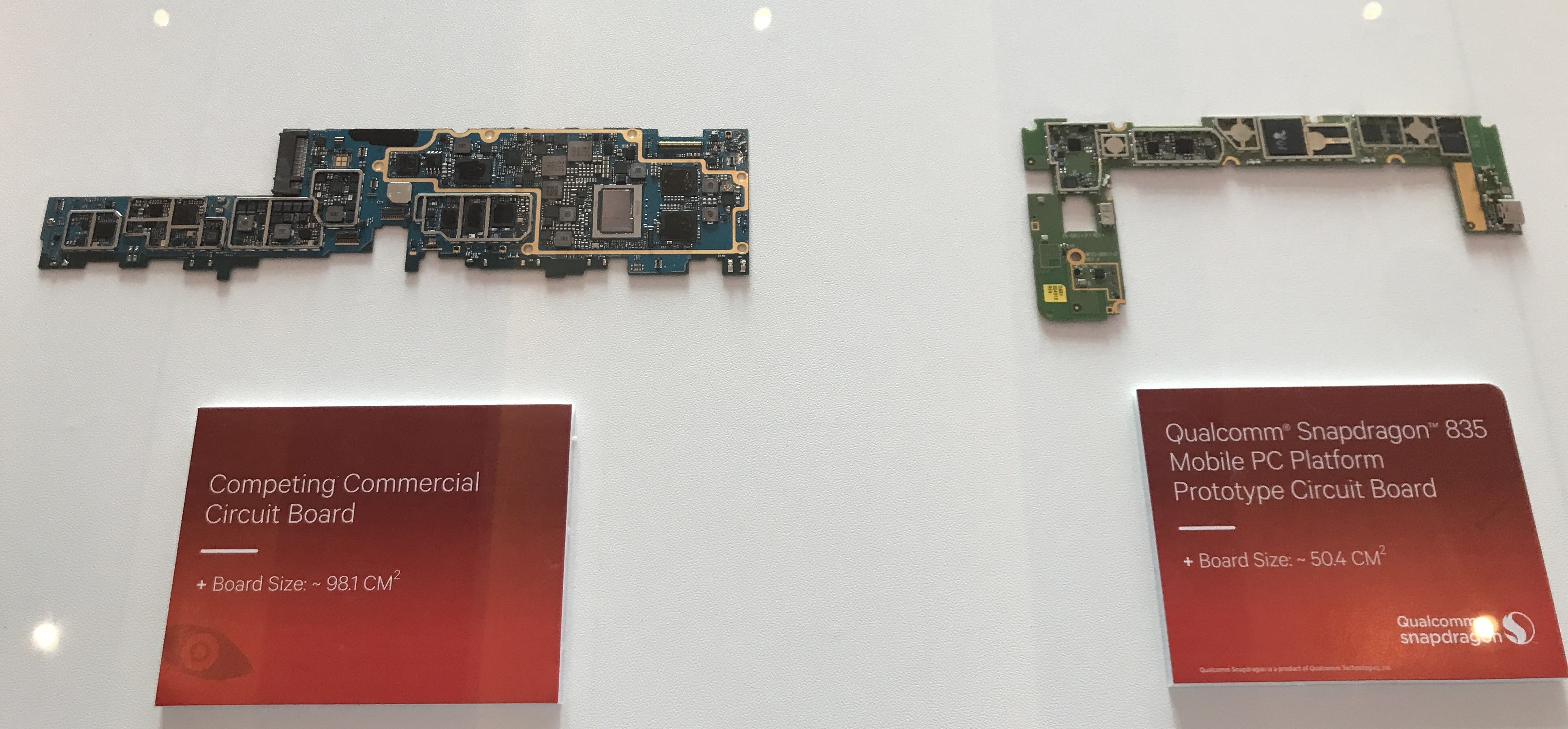
One of Qualcomm’s examples from 2018
For a Qualcomm processor designed for laptops, the silicon is a paired down to the essentials commonly associated with a smartphone. This means that modem connectivity is built into the processor, and the hardware associated with power delivery and USB are all on the scale of a smartphone. This means a motherboard designed around a Qualcomm processor will be around half the size, enabling different form factors, or more battery capacity in the same size laptop chassis.
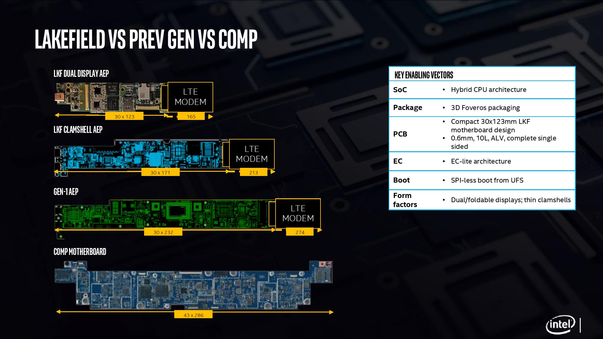
With Intel’s new Lakefield processor design, the chip is a lot smaller than previous Intel implementations. The company designed the processor from the ground up, with as much included on the CPU as to not need additional chips on the motherboard, and to fit the dimensions similar to one of Qualcomm’s processors. Above is a slide showing how Intel believes that with an LTE modem included, a Lakefield motherboard can move down to 7.7 square inches, similar to a Qualcomm design. This leaves more room for battery inside a device.
When Intel compares it against its own previous low power CPU implementations, the company quotes a 60% decrease in overall board area compared to its first generation 4.5 W processors.
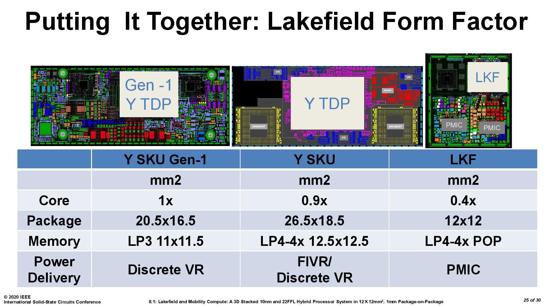
It is worth noting that for power delivery, Intel placed MIMCAPs inside the Lakefield silicon, much like a smartphone processor, and as a result it can get by on the power delivery implementation with a pair of PMICs (power management ICs). The reason why there is two is because of the two silicon dies inside – they are controlled differently for power for a number of technical reasons. If each layer within an active stacked implementation requires its own PMIC, that would presumably put an upper limit on future stacked designs – I fully expect Intel to be working on some sort of solution for this for it not to be an issue, however that wasn’t implemented in time for Lakefield.
For those that are interested, Lakefield’s PMICs are under the codenames Warren Cove and Castro Cover, and were developed in 2017-2018.


221 Comments
View All Comments
extide - Thursday, July 2, 2020 - link
That's basically what the latter generation Xeon Phi was.JorgeE1 - Thursday, July 2, 2020 - link
Intel can name the manufacturing process: Ferveros Ultra paCKed Scalar Hybrid Intel sTacked Silicon69369369 - Thursday, July 2, 2020 - link
EDGYD
G
Y
serendip - Thursday, July 2, 2020 - link
"But the bottom line is that in most cases, expect Lakefield to perform similar to four Atom cores, just above Goldmont Plus, and not like any of the Skylake/Ice Lake Core products and its derivatives."So a Kaby Lake Pentium will outperform this with 2 less cores and similar TDP while being a lot cheaper. That big core is sitting around doing nothing. It should be used as a turbo boost core, much like how the m3-8100Y behaves in the Surface Go 2.
Intel is either ballsy or stupid to pit this against the SD 8CX in the same price range.
lmcd - Thursday, July 2, 2020 - link
That TDP is at its pitiful base clocks. Tremont will outperform Sunny Cove and Skylake both at the lower power designations a second core is allowed, while using less die space. The second core in a Kaby Lake Pentium is worth less than the Tremont core in a theoretical 1+1 Lakefield design because the second core is throttled to around that 60% mark in the perf/watt curve graphic in the first place.Jorgp2 - Thursday, July 2, 2020 - link
Atom does support GFNIquorm - Thursday, July 2, 2020 - link
I don't know. The tech is interesting, especially the stacking, but overall, this doesn't seem to offer much benefit. Judging from the provided graphs, the power consumption difference between core and atom is too small to justify it. Does atom have dedicated hardware decode for current video codecs? Only way I could see this being beneficial, at least in this first iteration.brucethemoose - Thursday, July 2, 2020 - link
Even pure Atom SoCs had hardware decoding, right? IDK where it is on the die, but thats traditionally "part" of the GPU, and stuff like Netflix won't even run without it.lmcd - Thursday, July 2, 2020 - link
Yea that's 100% part of the die and it's why stuff like Silvermont getting upgraded Intel graphics as opposed to earlier bad PowerVR graphics (and weak decode blocks) was absolutely essentialalufan - Thursday, July 2, 2020 - link
hmm intel glueing cpus together then?Pity they are both sows ears and cant be polished