Arm's New Cortex-A78 and Cortex-X1 Microarchitectures: An Efficiency and Performance Divergence
by Andrei Frumusanu on May 26, 2020 9:00 AM EST- Posted in
- SoCs
- CPUs
- Arm
- Smartphones
- Mobile
- GPUs
- Cortex
- Cortex A78
- Cortex X1
- Mali G78
The Cortex-X1 Micro-architecture: Bigger, Fatter, More Performance
While the Cortex-A78 seems relatively tame in its performance goals, today’s biggest announcement is the far more aggressive Cortex-X1. As already noted, Cortex-X1 is a significant departure from Arm's usual "balanced" design philosophy, with Arm designing a core that favors absolute performance, even if it comes at the cost of energy efficiency and space efficiency.
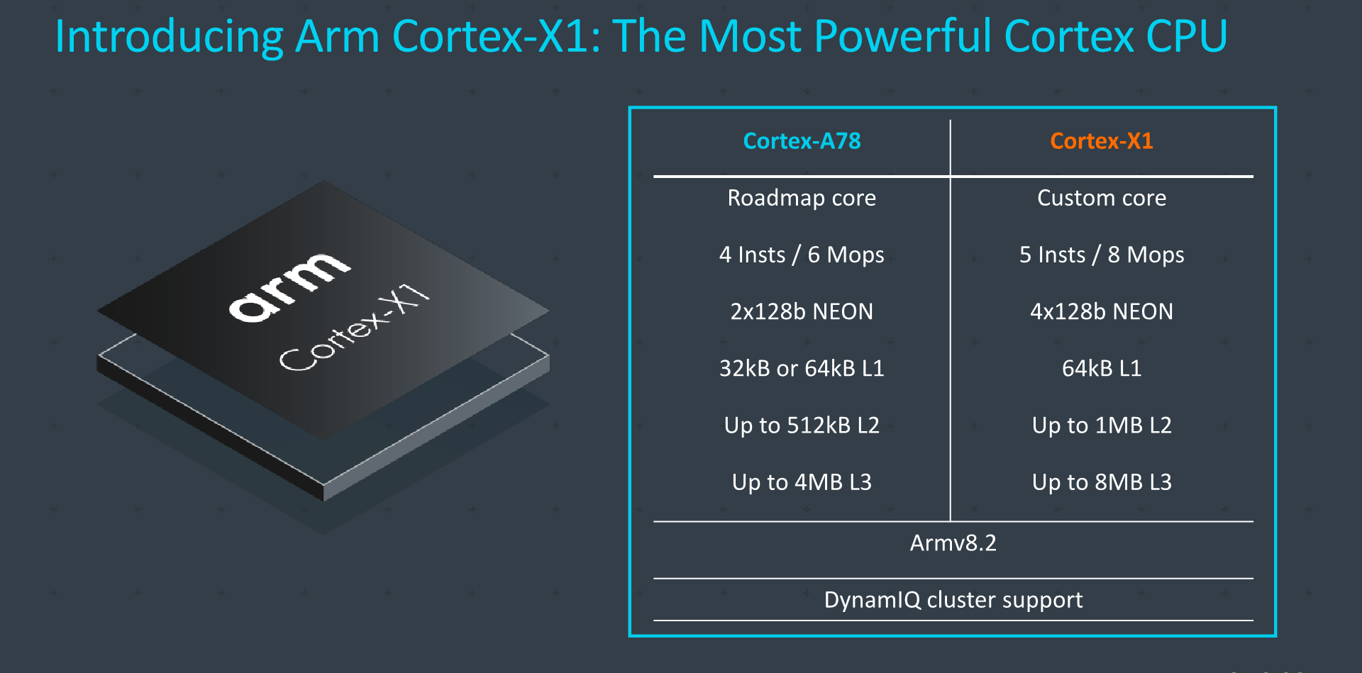
At a high level, the design could be summed up as being a ultra-charged A78 – maintaining the same functional principles, but increasing the structures of the core significantly in order to maximize performance.
Compared to an A78, it’s a wider core, going up from a 4- to a 5-wide decoder, increasing the renaming bandwidth to up to 8 Mops/cycle, and also vastly changing up some of the pipelines and caches, doubling up on the NEON unit, and double the L2 and L3 caches.
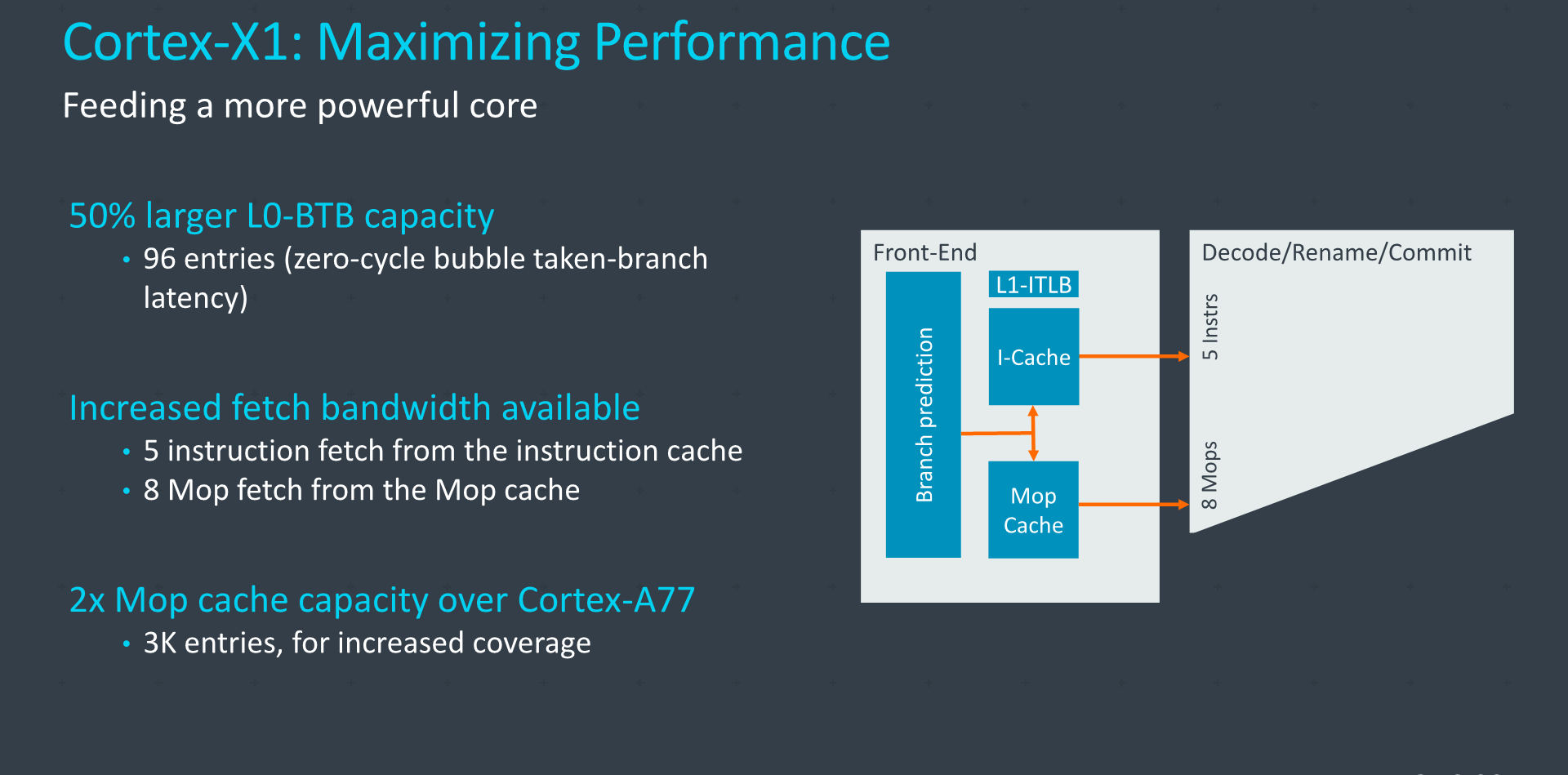
On the front-end (and valid the rest of the core as well), the Cortex-X1 adopts all the improvements that we’ve already covered on the Cortex-A78, including the new branch units. On top of the changes the A78 introduced, the X1 further grows some aspects of the blocks here. The L0 BTB has been upgraded from 64 entries on the Cortex-A77 and A78, to up to 96 entries on the X1, allowing for more zero latency taken branches. The branch target buffers are still of a two-tier hierarchy with the L0 and L2 BTBs, which Arm in previous disclosures referred to as the nanoBTB and mainBTB. The microBTB/L1 BTB was present in the A76 but had been subsequently discontinued.
The macro-op cache has been outright doubled from 1.5K entries to 3K entries, making this a big structure amongst the publicly disclosed microarchitectures out there, bigger than even Sunny Cove’s 2.25K entries, but shy of Zen2’s 4K entry structure - although we do have to make the disambiguation that Arm talks about macro-ops while Intel and AMD talk about micro-op caches.
The fetch bandwidth out of the L1I has been bumped up 25% from 4 to 5 instructions with a corresponding increase in the decoder bandwidth, and the fetch and rename bandwidth out of the Mop-cache has seen a 33% increase from 6 to 8 instructions per cycle. In effect, the core can act as a 8-wide machine as long as it’s hitting the Mop cache.
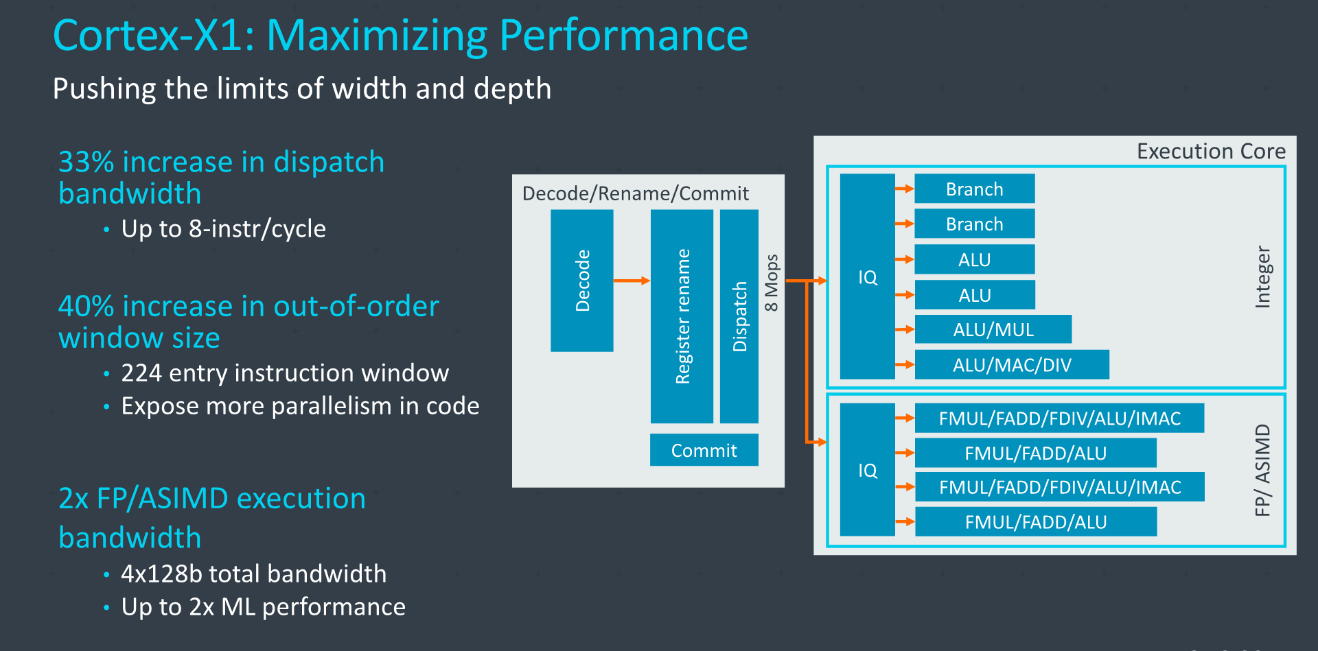
On the mid-core, Arm here again talks about increasing the dispatch bandwidth in terms of Mops or instructions per cycle, increasing it by 33% from 6 to 8 when comparing the X1 to the A78. In µops terms the core can handle up to 16 dispatches per cycle when cracking Mops fully into smaller µops, in that regard, representing a 60% increase compared to the 10µops/cycle the A77 was able to achieve.
The out-of-order window size has been increased from 160 to 224 entries, increasing the ability for the core to extract ILP. This had always been an aspect Arm had been hesitant to upgrade as they had mentioned that performance doesn’t scale nearly as linearly with the increased structure size, and it comes at a cost of power and area. The X1 here is able to make those compromises given that it doesn’t have to target an as wide range of vendor implementations.
On the execution side, we don’t see any changes on the part of the integer pipelines compared to the A78, however the floating point and NEON pipelines more significantly diverge from past microarchitectures, thanks to the doubling of the pipelines. Doubling here can actually be taken in the literal sense, as the two existing pipelines of the A77 and A78 are essentially copy-pasted again, and the two pairs of units are identical in their capabilities. That’s a quite huge improvement and increase in execution resources.
In effect, the Cortex-X1 is now a 4x128b SIMD machine, pretty much equal in vector execution width as some desktop cores such as Intel’s Sunny Cove or AMD’s Zen2. Though unlike those designs, Arm's current ISA doesn't allow for individual vectors to be larger than 128b, which is something to be addressed in a next generation core.
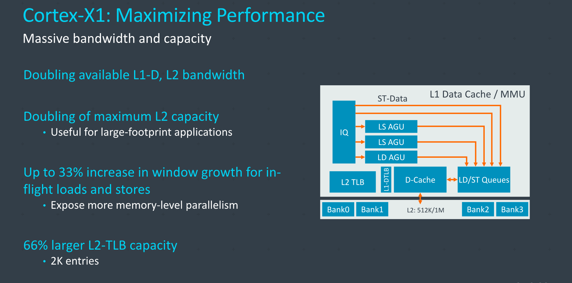
On the memory subsystem side, the Cortex-X1 also sees some significant changes – although the AGU setup is the same as that found on the Cortex-A78.
On the part of the L1D and L2 caches, Arm has created new designs that differ in their access bandwidth. The interfaces to the caches here aren’t wider, but rather what’s changed is the caches designs themselves, now implementing double the memory banks. What this solves is possible bank conflicts when doing multiple concurrent accesses to the caches, it’s something that we may have observed with odd “zig-zag” patterns in our memory tests of the Cortex-A76 cores a few years back, and still present in some variations of that µarch.
The L1I and L1D caches on the X1 are meant to be configured at 64KB. On the L2, because it’s a brand new design, Arm also took the opportunity to increase the maximum size of the cache which now doubles up to 1MB. Again, this actually isn’t the same 1MB L2 cache design that we first saw on the Neoverse-N1, but a new implementation. The access latency is 1 cycle better than the 11-cyle variant of the N1, achieving 10 cycles on the X1, regardless of the size of the cache.
The memory subsystem also increases the capability to support more loads and stores, increasing the window here by 33%, adding even more onto the MLP ability of the core. We have to note that this increase not merely refers to the store and load buffers but the whole system’s capabilities with tracking and servicing requests.
Finally, the L2 TLB has also seen a doubling in size compared to the A78 (66% increase vs A77) with 2K entries coverage, serving up to 8MB of memory at 4K pages, which makes for a good fit for the envisioned 8MB L3 cache for target X1 implementations.
The doubling of the L3 cache in the DSU doesn’t necessarily mean that it’s going to be a slower implementation, as the latency can be the same, but depending on partner implementations it can mean a few extra cycles of latency. Likely what this is referring to is likely the option for banking the L3 with separated power management. To date, I haven’t heard of any vendors using this feature of the DSU as most implementers such as Qualcomm have always had the 4MB L3 fully powered on all the time. It is possible that with a 8MB DSU that some vendors might look into power managing this better, for example it having being only partially powered on as long as only little cores are active.
Overall, what’s clear here about the Cortex-X1 microarchitecture is that it’s largely consisting of the same fundamental building blocks as that of the Cortex-A78, but only having bigger and more of the structures. It’s particularly with the front-end and the mid-core where the X1 really supersizes things compared to the A78, being a much wider microarchitecture at heart. The arguments about the low return on investment on some structures here just don’t apply on the X1, and Arm went for the biggest configurations that were feasible and reasonable, even if that grows the size of the core and increases power consumption.
I think the real only design constraints the company set themselves here is in terms of the frequency capabilities of the X1. It’s still a very short pipeline design with a 10-cycle branch mispredict penalty and a 13-stage deep frequency design, and this remains the same between the A78 and X1, with the latter’s bigger structures and wider design not handicapping the peak frequencies of the core.


192 Comments
View All Comments
DanNeely - Tuesday, May 26, 2020 - link
having gotten to page 4 in the article, the explanation is that ARMs slides as used on the first page suck. The 20% from A77-A78 is +7% architecture, and +13% 5nm instead of 7nm. The 30% from A77-X1 is entirely architecture; that in turn implies that upcoming X1 chips should be about 40-45% faster than current A77 ones.AIUI It's still going to be falling short of what Apple's doing (and not just because the A55 little cores are getting really dated); but is a badly needed narrowing of the gap.
ichaya - Tuesday, May 26, 2020 - link
40-45% on appropriately less die area than Apple and you've got something competitive atleast.DanNeely - Tuesday, May 26, 2020 - link
in terms of engineering prowess certainly; but not in terms of letting Samsung/etc finally design smartphones and tablets that are as fast as their rivals from Apple. Assuming the product plays out in retail, in another 2 or 3 years when I look to replace my S10 I'll probably get something with an X core in it; but I really hope that they'll widen the performance uplift vs their more general purpose cores by then.Raqia - Tuesday, May 26, 2020 - link
The existing A77's are already very impressive in terms of PPA, I would consider them as impressive as Apple's big cores taken as a whole. (The small cores are another story since the major uplift from the A13...) A lot of Android vendors value area in particular since they integrate modems on die whereas Apple does not; this drives a lot of value and cost savings for customers.CiccioB - Tuesday, May 26, 2020 - link
If Samsung really wants to create a phone/tablet as fast as an Apple one it should first concentrate more on SW optimizations. Apple puts a lot of efforts in that. It's not only a question who makes the bigger core.See the comparison of Samsung crappy phones with other Android ones using much more optimized and less bloated version of the OS. They are good for benchmarking with all those cores and MHz (and tricks on turbo spped for benchmark apps), but in real life Samsung phones are slower than they could be do to low optimizations.
Wilco1 - Tuesday, May 26, 2020 - link
Bingo! Adding a big core that does well in benchmarks is not a good solution. Improving browser performance with software optimization can be far more effective.armchair_architect - Wednesday, May 27, 2020 - link
@Wilco1 I am afraid you only the SW part of the equation here.Again X1 is not only good in benchmarks, being wide helps in that you can achieve same performance as last-gen by running at vastly lower frequency and voltage.
Thus power efficiency for all use cases that do not require max peak perf enjoy a huge power saving.
Wilco1 - Thursday, May 28, 2020 - link
You can't brute-force your way to performance or efficiency. If you can improve performance via software optimization, you take it any time over a faster core that gives the same gain but needs more power to run the unoptimized software.It's as simple as that.
armchair_architect - Thursday, May 28, 2020 - link
Obviously you would ideally need both SW optimization and faster CPUs.But again, power will not always be higher and higher power != higher energy usage.
Wilco1 - Thursday, May 28, 2020 - link
Absolutely. But the biggest issue in the Android world is software optimization and tuning, not CPU performance. Improving that would easily add up to a new CPU generation. The choice to switch to LLVM was stupid at the time, but even more so today since GCC has since moved further ahead of LLVM...Note all the evidence points to using smaller cores to improve power efficiency. You can see this on the perf/W estimates for SPEC - the A78 is almost twice as efficient as A13 while achieving 74% of the performance.