The Samsung Galaxy S10+ Snapdragon & Exynos Review: Almost Perfect, Yet So Flawed
by Andrei Frumusanu on March 29, 2019 9:00 AM ESTMemory Subsystems Compared - Bandwidth & MLP
While memory latency is one part of the story, the other aspect of memory performance is memory bandwidth. In order to test this out I expanded the memory testing tools with tests which also stressed this part of the CPU. The patterns here are quite simple: pure linear bandwidth using SIMD units. In the case of the Arm chips this means 128b NEON instructions while as a comparison data-point the Intel data is using 128b and 256b AVX/AVX2 instructions. The published figures use the STREAM convention, meaning the amount of data that the code explicitly reads and writes.
- ST: pure store bandwidth, we’re just writing static data into memory
- LD: pure load bandwidth, the data here is volatile and we’re merely reading data into registers without doing anything with it
- Flip: Consisting of load and store instructions, within a cache line we flip the words around while flipping the whole data array around on itself on a cache-line basis. Essentially this is exactly the same bandwidth as a memory copy, it’s just that we’re staying within a set memory region.
- CLflip / cache-line flip: We’re flipping the words within cache lines around.
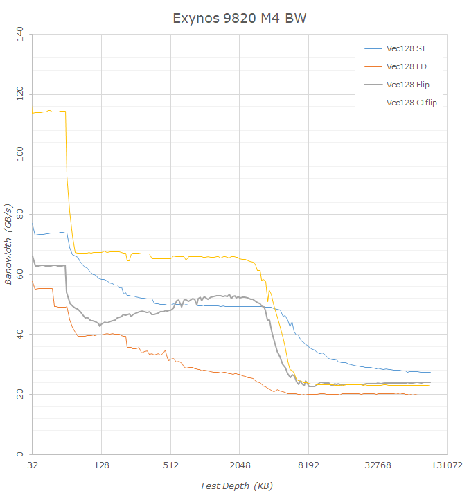
Starting off again with a look at how the new Exynos M4 Cheetah cores compare to last year’s M3 Meerkat, we see that Samsung has significantly improved the bandwidth of the core. Indeed one of the bigger microarchitectural changes of the core was the addition of a second data store unit. To be more precise, one of the prior two load units was converted into a load/store unit, which in theory doubles the store bandwidth of the core. Looking at the data this is confirmed by the L1 store bandwidth which jumps from 36GB/s to 74GB/s. However the improvements look not to be only limited to the store bandwidth as the load bandwidth also increases from 36GB/s to 58GB/s. Memory flip/copy bandwidth on the L1 increases by essentially ~50% from 43GB/s to 66GB/s.
What is odd to see is that flip bandwidth is lower in the L2 cache than it is in the L3, something we also saw in the Exynos 9810. When looking at the different memory bandwidth curves, in particular the store bandwidth of the M3 and M4, we see that in the L3 memory region store curve is actually offset by 1MB compared to the flip/load curves, which ending only after 3MB. That’s bit of an odd thing to explain but reinforces the notion that Samsung is using 1MB of the L3 in a different way. DRAM flip/copy bandwidth increases from 19.5GB/s to 24GB/s which is a little better than the theoretical increase from moving from 1794MHz memory to the 2093MHz used in the new Galaxy S10.
The Snapdragon 855 versus the Snapdragon 845 also sees some big improvements, however the comparison to the A75 might be a bit flawed as the CPU only had a single 128b NEON pipeline and thus it’s possible we’re not really stressing the cache hierarchy at its maximum, with the numbers possibly being lower than what they could be in the L1 and L2 part of the bandwidth curves.
What is really odd to see is the flip/copy behaviour on the new Cortex A76 cores. This zig-zagging pattern also happens on the Kirin 980 and seems to be a characteristic of the microarchitecture, probably some cache-bank access conflict.
The one thing that the Snapdragon 855 differs significantly in compared to the Kirin 980 is the flip/copy bandwidth in the L3 and above, here we see a 50% advantage on the part of the Snapdragon 855 and this continues on into DRAM bandwidth with 21.4GB/s for the Snapdragon versus a meagre 11.7GB/s on the HiSilicon chipset. It’s to be noted that this is indeed near the theoretical bandwidth of the memory controllers at 33.4GB. We’re only measuring 21.4GB/s because this is the STREAM convention bandwidth and not what the hardware is actually doing, in the case of a memory copy the CPU would first read out the contents of the target buffer cacheline before writing into it, meaning the hardware bandwidth would be 50% higher (2 loads 1 store for a memory copy location).
It’s possible to avoid this second memory load when using non-temporal memory stores. Such a mechanism didn’t exist for the ARM ISA prior to ARMv8, but has been around for a while in x86. What is interesting to see is that the new M4 and Cortex A76 pure memory stores essentially behave as non-temporal stores in this test, taking advantage of the ISA’s more relaxed memory model. The store bandwidth in DRAM thus reaches near the theoretical maximum DRAM memory bandwidth with 27.4GB-28GB/s for the Exynos M4 and Cortex A76 in both the Kirin and Snapdragon chipsets. Intel’s 9900K here has to read out the memory location before writing to it, thus only reaches half the theoretical peak of DDR4-3200 at 18GB/s – it’s only with explicit non-temporal store instructions that the Intel core achieves similar behaviour to the new Arm cores. It’s to be noted that Apple’s cores also behave more like Intel’s in this case, showing only 13.9GB/s store bandwidth and also a lower 17.9GB/s flip/copy bandwidth.

The memory bandwidth tests also expose an interesting bottleneck on the part of the Cortex A75 cores inside the Exynos 9820. Here, we see some atrocious performance dip in the L3 memory region. The same test in the Snapdragon 845 with the CPU cores integrated into Arm’s own DSU doesn’t showcase anything anywhere similar to this, so it must be something related to how Samsung has integrated the CPU cores into their own proprietary cluster design. Simultaneous read/writes into the same cache line shouldn’t be all that common in the real-world so it’s unclear exactly how this would impact the CPU’s performance, it does however also show up as a smaller dip in the copy bandwidth of the core.
Memory Level Parallelism
Memory level parallelism (MLP) probably isn’t talked about as much as it should, and we ought to cover the topic more. Last year during the Cortex A76 Tech Day coverage one topic Arm kept mentioning is how its MLP capabilities have massively improved in the new design.
MLP describes multiple accesses to different memory locations, in this context we’re talking about purely single-threaded MLP, meaning a CPU core’s ability to deal with multiple data accesses. If data isn’t located in a CPU’s cache hierarchy it means we have a data miss, however when this happens out-of-order CPUs don’t just merely wait around for the memory access to be fulfilled, but rather go on executing other instructions which aren’t blocked. Exactly how many such data misses the CPU can deal with is called the outstanding miss capability. Traditionally such misses are tracked by miss status holding registers (MSHRs), however I haven’t seen Arm CPUs actually use this nomenclature.
Creating a test for MLP I was inspired by Daniel Lemire’s blog post on the matter and subsequent post on the Apple A12. I integrated a similar concept into my test suite, however took a different approach in regards to the data, adding an extremely important third axis to the data, access depth.
The MLP test here is related to the “Full Random” latency test on the previous page, meaning we’re dealing a chain of random pointers. The difference here is that I’m distributing at equal node distance multiple starting points within the test chain, and traversing it in parallel, scaling up with access pointers (MLP depth).
What is important to note here is that we’re looking just at one aspect of MLP, this being combined core TLB and cache outstanding miss capacity. The data presented is the normalised speedup versus the single-access latency of the full random chain. The Y axis is the speedup factor, while the stacked lines represent the results of the incrementing parallel accesses.
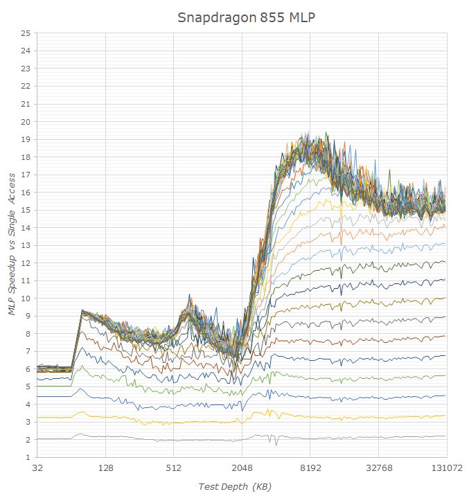
Looking at the Snapdragon 855 first, we indeed see some massive improvements in MLP capability on the part of the Cortex A76 cores, in particular when compared to the prior generation A75 cores. I was actually extremely surprised to see the A75 fare so badly, especially in the L2 region, as the core seemingly is only able to deal with 2-3 outstanding misses. In particular it’s interesting to see that in the L3 region, the A75 cores of the Exynos 9820 fare much better than the same cores in the Snapdragon 845, meaning on the latter chip we might be seeing actual limits in terms of concurrent accesses on the part of the cache.
The new A76 seems to be able to handle 8 outstanding misses to the L2, and we see similar results for of both the Snapdragon 855 as well as Kirin 980. The new core’s MLP capabilities performance on the DRAM side is quite impressive as it seems to handle a peak of 20 outstanding misses and actually sustain 15-16 in deeper memory depths without issues, with also quite linear scaling between MLP depth and actual access speedup.
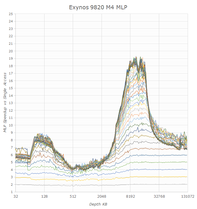
Looking at the Exynos 9820’s performance, we’re seeing some very big differences to Arm’s newest A76. Indeed even looking back at the Exynos 9810 we see behaviour that reminds us of the TLB issues we saw earlier in the latency analysis: Both the M3 and the new M4’s performance collapses after exceeding the microTLB capacity. Because we’re seeing that on the Exynos 9820’s A75 cores that the L3 cache seemingly is able to handle ~12 outstanding requests, the M3’s and M4’s inability to handle more than 5-6 misses in this region must be inherently tied to a lack of parallelism on the part of the TLB units on Samsung’s cores. When looking at DRAM outstanding misses it does look like the core can handle 32 misses, however once we’re out of the L2 TLB capacity this again quickly collapses to 7-8 requests. This discrepancy between Samsung’s cores and the new Cortex A76 in the deeper DRAM regions would mean that the actual hardware page table walker on Arm’s cores is able to service double the amount of requests.
It’s also interesting to see how other CPU cores perform in this test. Apple’s A12 Vortex seems to be the outright leader in terms of handling outstanding requests, able to fulfill ~21 requests to the L2 cache and ~41 to DRAM. What is weird is that the A12's speedup scaling is that it isn’t as clean and linear as other cores, and in particular there’s a very weird performance jump from 20 to 21 and 40 to 41 requests which I haven’t found a convincing explanation for yet. It’s also interesting to see what appears to be the last level TLB of the Vortex cores at 2048 pages / 128MB capacity.
On the part of the desktop cores Intel is doing well at ~12 outstanding misses to L2 and 20 to L3, although it can only sustain ~16 which looks to be the TLB limitation. We don’t have the graphs published in this piece but AMD’s Zen does the best in the lower cache hierarchies with a rock steady 16 outstanding misses to L2 and ~30-32 misses to L3 with a 22x speedup and sustaining ~20 to DRAM with a 14-16x speedup.
Overall the Snapdragon and Cortex A76 look to perform extremely well in the MLP aspect and the core does look to bring big improvements in this regard compared to previous generation Arm cores. With this test we’re also exposing some of Samsung’s CPU core bottlenecks – in particular the TLBs seem to be problematic as we’re seeing both latency as well and parallel access limitations that aren’t as pronounced in other cores. The weird memory bandwidth behaviour on the Cortex A75 cores in the Exynos 9820 also points out that the custom design has some rough edges that hopefully will be sorted out in future generations.


229 Comments
View All Comments
luca.costantino - Friday, March 29, 2019 - link
Way too much bloatware on Samsung products for my taste. I would never consider buying a phone from them.shabby - Friday, March 29, 2019 - link
Are you offended or something? That's the dumbest comment I ever read, I just sold an s9 and wiped it, the buyer said I thought it would have more bloatware but it doesn't.liteon163 - Friday, March 29, 2019 - link
No need to be so harsh simply because you disagree with someone's opinion, dude. Don't be a jerk (that's not an opinion, that's a FACT proven by your initial reply).close - Sunday, March 31, 2019 - link
Samsung has their own equivalent of every single piece of software that comes with Android and you already didn't want in your phone. @shabby just wanted to tell us he knows how to follow a decrapify tutorial. The phone is still crappy software-wise but after putting in a lot of effort you can make it marginally less crappy. Yay?Vermite - Sunday, May 19, 2019 - link
You're an idiot. Yay?s.yu - Sunday, March 31, 2019 - link
There are smarter opinions and stupider opinions.goatfajitas - Friday, March 29, 2019 - link
Yes, it does have alot of bloat.mazook - Friday, March 29, 2019 - link
Dude, the ROM is about 4 GIGS.Think there's just a BIT of bloat in there?
Samus - Sunday, March 31, 2019 - link
I figured Android users are just used to bloat at this point. I’d you want a clean optimized mobile experience you either buy a Google phone, install a 3rd party ROM, or just buy an iPhone.notashill - Monday, April 1, 2019 - link
The "bloatware free" Android One ROMs are like 12 gigs though they do keep 2 entire copies of the system partition for the seamless update feature. Very annoying especially considering how many Android One devices have 32GB storage.