Arm's New Cortex-A78 and Cortex-X1 Microarchitectures: An Efficiency and Performance Divergence
by Andrei Frumusanu on May 26, 2020 9:00 AM EST- Posted in
- SoCs
- CPUs
- Arm
- Smartphones
- Mobile
- GPUs
- Cortex
- Cortex A78
- Cortex X1
- Mali G78
The Cortex-X1 Micro-architecture: Bigger, Fatter, More Performance
While the Cortex-A78 seems relatively tame in its performance goals, today’s biggest announcement is the far more aggressive Cortex-X1. As already noted, Cortex-X1 is a significant departure from Arm's usual "balanced" design philosophy, with Arm designing a core that favors absolute performance, even if it comes at the cost of energy efficiency and space efficiency.
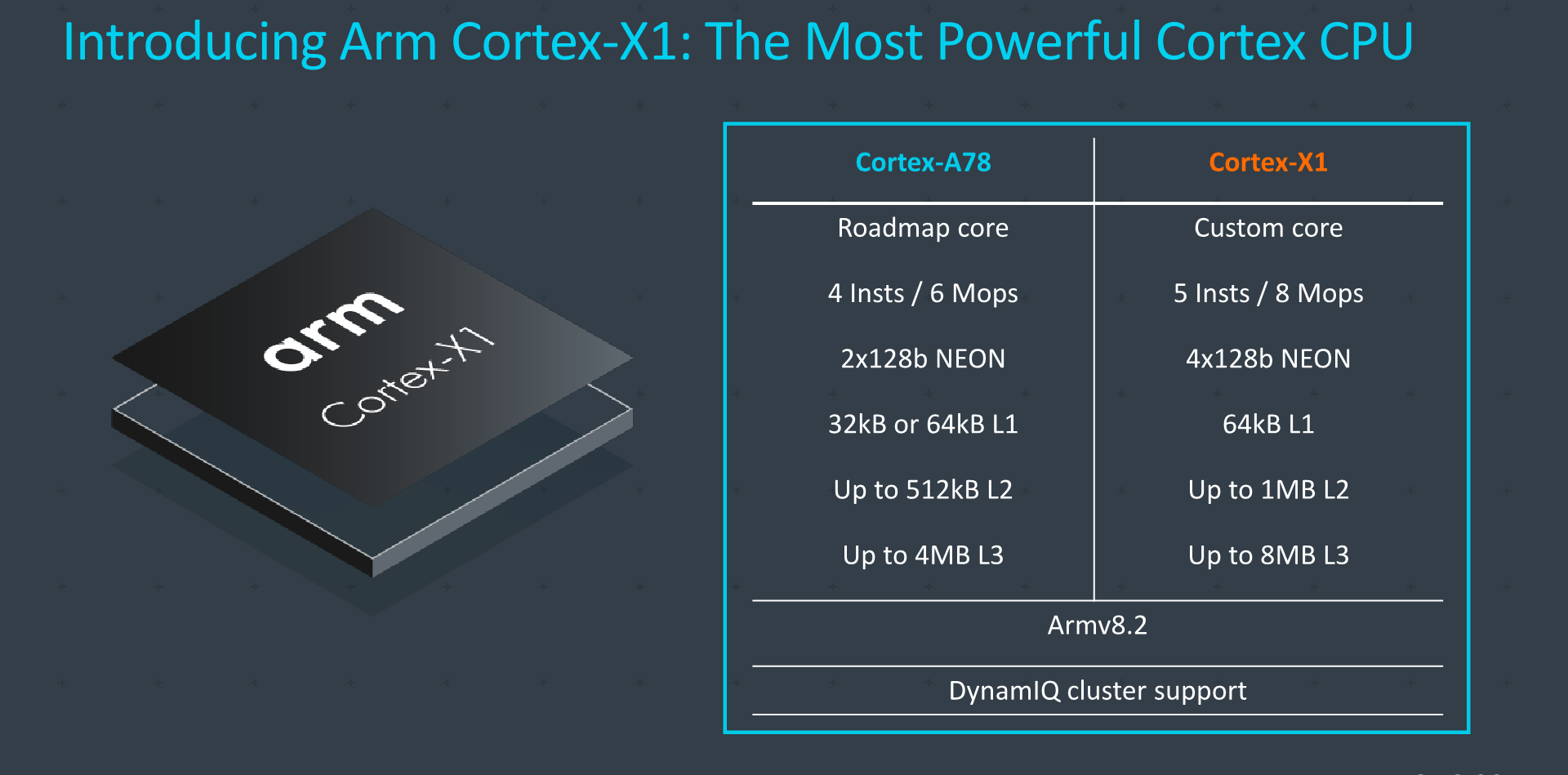
At a high level, the design could be summed up as being a ultra-charged A78 – maintaining the same functional principles, but increasing the structures of the core significantly in order to maximize performance.
Compared to an A78, it’s a wider core, going up from a 4- to a 5-wide decoder, increasing the renaming bandwidth to up to 8 Mops/cycle, and also vastly changing up some of the pipelines and caches, doubling up on the NEON unit, and double the L2 and L3 caches.
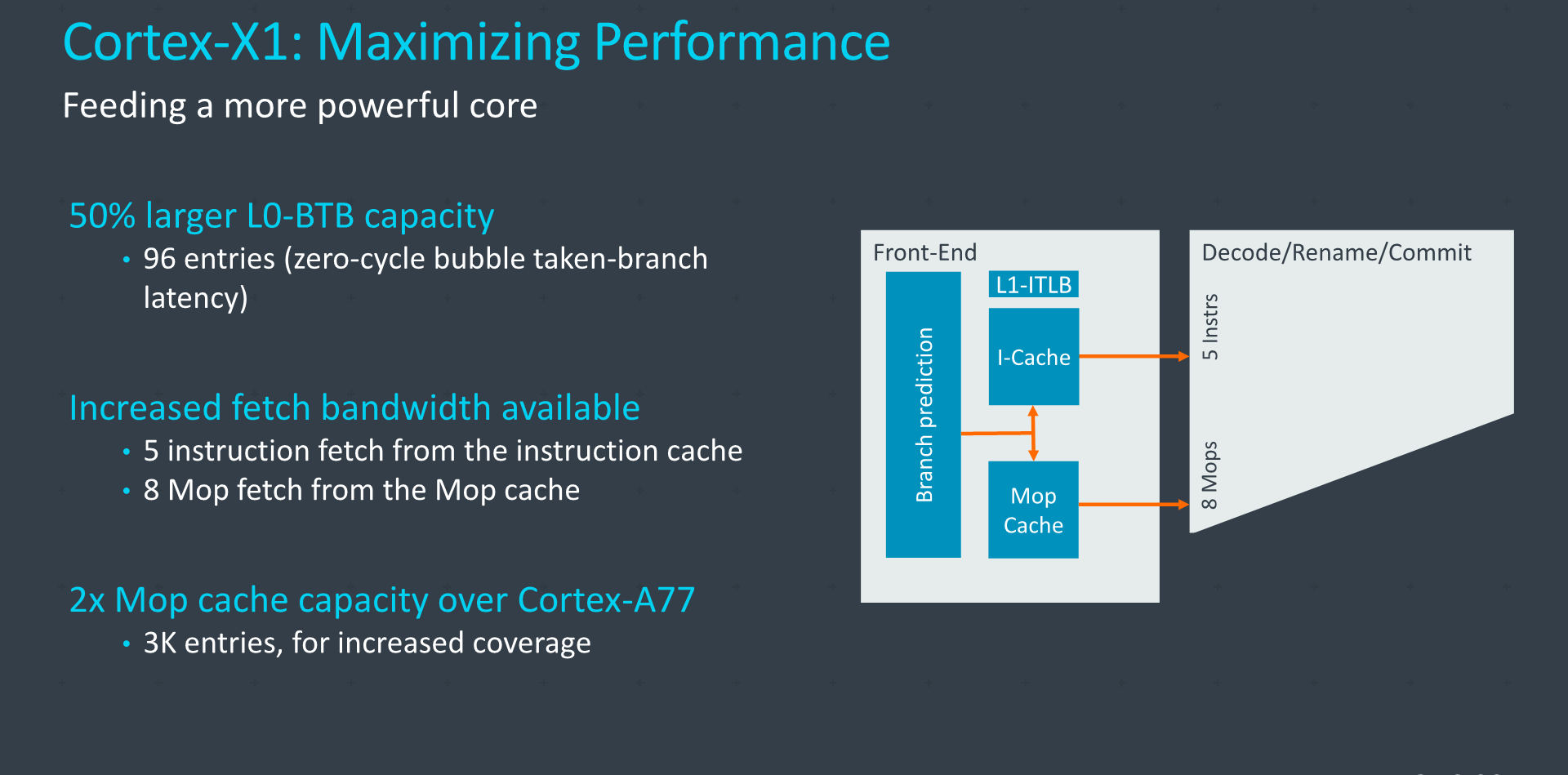
On the front-end (and valid the rest of the core as well), the Cortex-X1 adopts all the improvements that we’ve already covered on the Cortex-A78, including the new branch units. On top of the changes the A78 introduced, the X1 further grows some aspects of the blocks here. The L0 BTB has been upgraded from 64 entries on the Cortex-A77 and A78, to up to 96 entries on the X1, allowing for more zero latency taken branches. The branch target buffers are still of a two-tier hierarchy with the L0 and L2 BTBs, which Arm in previous disclosures referred to as the nanoBTB and mainBTB. The microBTB/L1 BTB was present in the A76 but had been subsequently discontinued.
The macro-op cache has been outright doubled from 1.5K entries to 3K entries, making this a big structure amongst the publicly disclosed microarchitectures out there, bigger than even Sunny Cove’s 2.25K entries, but shy of Zen2’s 4K entry structure - although we do have to make the disambiguation that Arm talks about macro-ops while Intel and AMD talk about micro-op caches.
The fetch bandwidth out of the L1I has been bumped up 25% from 4 to 5 instructions with a corresponding increase in the decoder bandwidth, and the fetch and rename bandwidth out of the Mop-cache has seen a 33% increase from 6 to 8 instructions per cycle. In effect, the core can act as a 8-wide machine as long as it’s hitting the Mop cache.
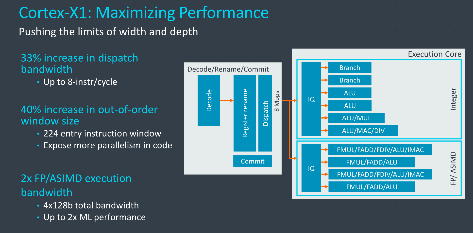
On the mid-core, Arm here again talks about increasing the dispatch bandwidth in terms of Mops or instructions per cycle, increasing it by 33% from 6 to 8 when comparing the X1 to the A78. In µops terms the core can handle up to 16 dispatches per cycle when cracking Mops fully into smaller µops, in that regard, representing a 60% increase compared to the 10µops/cycle the A77 was able to achieve.
The out-of-order window size has been increased from 160 to 224 entries, increasing the ability for the core to extract ILP. This had always been an aspect Arm had been hesitant to upgrade as they had mentioned that performance doesn’t scale nearly as linearly with the increased structure size, and it comes at a cost of power and area. The X1 here is able to make those compromises given that it doesn’t have to target an as wide range of vendor implementations.
On the execution side, we don’t see any changes on the part of the integer pipelines compared to the A78, however the floating point and NEON pipelines more significantly diverge from past microarchitectures, thanks to the doubling of the pipelines. Doubling here can actually be taken in the literal sense, as the two existing pipelines of the A77 and A78 are essentially copy-pasted again, and the two pairs of units are identical in their capabilities. That’s a quite huge improvement and increase in execution resources.
In effect, the Cortex-X1 is now a 4x128b SIMD machine, pretty much equal in vector execution width as some desktop cores such as Intel’s Sunny Cove or AMD’s Zen2. Though unlike those designs, Arm's current ISA doesn't allow for individual vectors to be larger than 128b, which is something to be addressed in a next generation core.
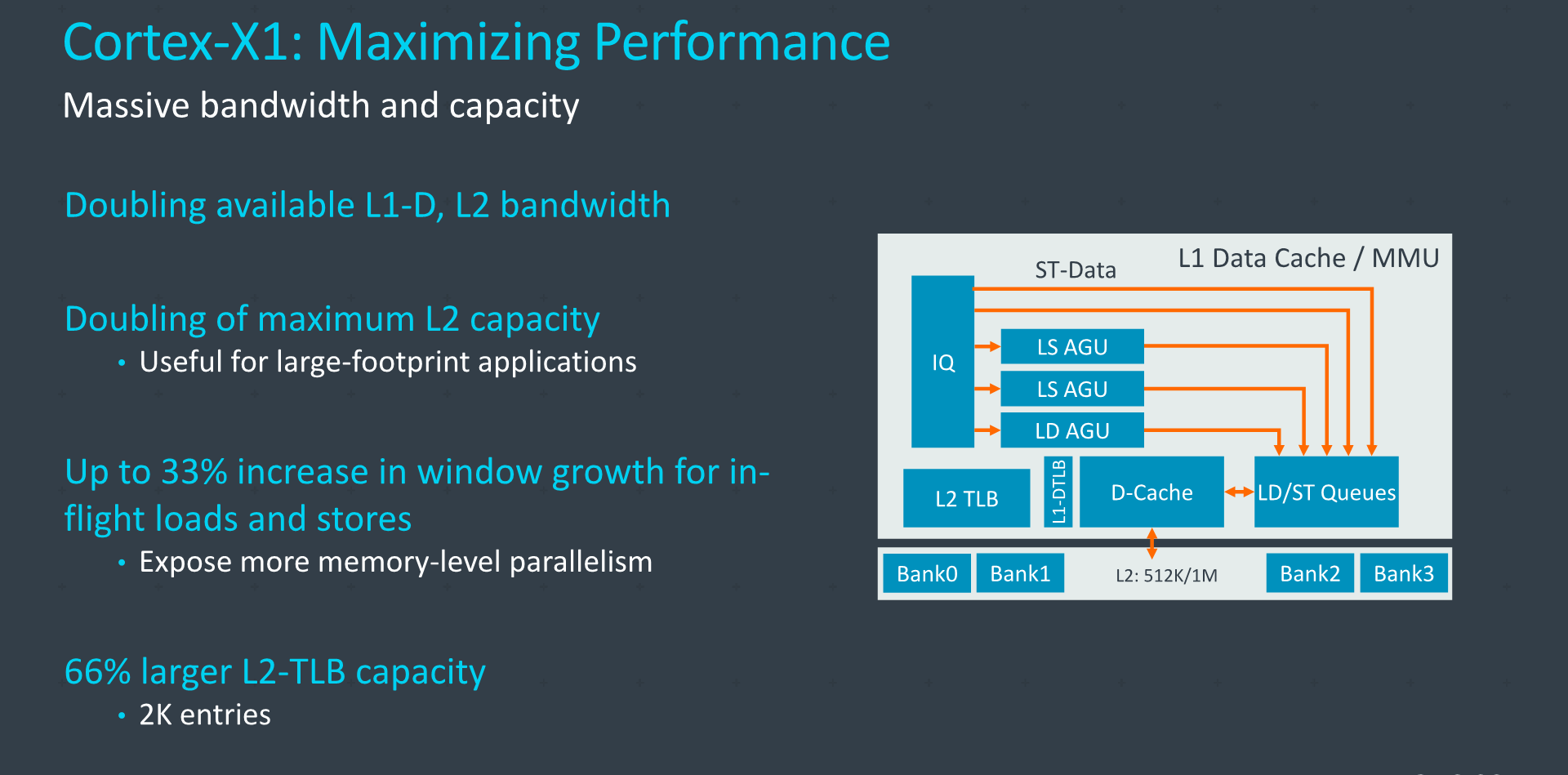
On the memory subsystem side, the Cortex-X1 also sees some significant changes – although the AGU setup is the same as that found on the Cortex-A78.
On the part of the L1D and L2 caches, Arm has created new designs that differ in their access bandwidth. The interfaces to the caches here aren’t wider, but rather what’s changed is the caches designs themselves, now implementing double the memory banks. What this solves is possible bank conflicts when doing multiple concurrent accesses to the caches, it’s something that we may have observed with odd “zig-zag” patterns in our memory tests of the Cortex-A76 cores a few years back, and still present in some variations of that µarch.
The L1I and L1D caches on the X1 are meant to be configured at 64KB. On the L2, because it’s a brand new design, Arm also took the opportunity to increase the maximum size of the cache which now doubles up to 1MB. Again, this actually isn’t the same 1MB L2 cache design that we first saw on the Neoverse-N1, but a new implementation. The access latency is 1 cycle better than the 11-cyle variant of the N1, achieving 10 cycles on the X1, regardless of the size of the cache.
The memory subsystem also increases the capability to support more loads and stores, increasing the window here by 33%, adding even more onto the MLP ability of the core. We have to note that this increase not merely refers to the store and load buffers but the whole system’s capabilities with tracking and servicing requests.
Finally, the L2 TLB has also seen a doubling in size compared to the A78 (66% increase vs A77) with 2K entries coverage, serving up to 8MB of memory at 4K pages, which makes for a good fit for the envisioned 8MB L3 cache for target X1 implementations.
The doubling of the L3 cache in the DSU doesn’t necessarily mean that it’s going to be a slower implementation, as the latency can be the same, but depending on partner implementations it can mean a few extra cycles of latency. Likely what this is referring to is likely the option for banking the L3 with separated power management. To date, I haven’t heard of any vendors using this feature of the DSU as most implementers such as Qualcomm have always had the 4MB L3 fully powered on all the time. It is possible that with a 8MB DSU that some vendors might look into power managing this better, for example it having being only partially powered on as long as only little cores are active.
Overall, what’s clear here about the Cortex-X1 microarchitecture is that it’s largely consisting of the same fundamental building blocks as that of the Cortex-A78, but only having bigger and more of the structures. It’s particularly with the front-end and the mid-core where the X1 really supersizes things compared to the A78, being a much wider microarchitecture at heart. The arguments about the low return on investment on some structures here just don’t apply on the X1, and Arm went for the biggest configurations that were feasible and reasonable, even if that grows the size of the core and increases power consumption.
I think the real only design constraints the company set themselves here is in terms of the frequency capabilities of the X1. It’s still a very short pipeline design with a 10-cycle branch mispredict penalty and a 13-stage deep frequency design, and this remains the same between the A78 and X1, with the latter’s bigger structures and wider design not handicapping the peak frequencies of the core.


192 Comments
View All Comments
name99 - Saturday, May 30, 2020 - link
Yes yes yes, eternal evil Apple not allowing people to do what they want. We all know the story.Meanwhile, in the real world:
https://support.apple.com/en-gb/HT202655
Vince789 - Friday, May 29, 2020 - link
Not surprising as a $1500 Exynos S20 Ultra is slower than a $400-500 865 phones tooSamus - Wednesday, May 27, 2020 - link
I think syxbit's disappointment is rooted in that a current $400 Apple device available right now will probably be faster than this chip, whenever it is available, and will likely only be in much more expensive phones.That is incredibly disappointing. Especially when you consider Android has a native performance penalty in UI performance and overall optimization due to its broad hardware compatibility requirements. If anything, Android should be getting the faster chips since Apple has the luxury of optimizing their OS around their SoC.
Lolimaster - Wednesday, May 27, 2020 - link
$400 Apple SOC on a 2015 "value" body.All around the K30 Pro Zoom rubs circles around it as a modern device. My 5.8" S9 can feel quite small for media consumption, browsing and gaming. Can't imagine something well below 5" as a "smartphone" in 2020.
Spunjji - Thursday, May 28, 2020 - link
"...Android has a native performance penalty in UI performance..."Somebody has clearly never used a OnePlus device..!
Apple having a theoretically faster CPU makes no difference if:
1) Apple won't sell that CPU to anyone else
2) Apple won't use anyone else's CPUs
3) You care about the actual experience you get form the device, not benchmarks.
iphonebestgamephone - Friday, May 29, 2020 - link
I currently use a oneplus, the ui animation does look better on iphones, oneplus is just sped up animations - slowing it down doesnt make it look better either.darkich - Wednesday, May 27, 2020 - link
For years now, iPhones are CONSISTENTLY inferior to the Samsung Galaxy S phones in the best and most objective real life speed tests.Go see phonebuff channel and educate yourself.
iphonebestgamephone - Wednesday, May 27, 2020 - link
Ah yes, the app open tests. Wonderful indeed.jospoortvliet - Thursday, May 28, 2020 - link
you missed the sarcasm tag ;-)But yeah, those "real world tests", comparing the animation speeds of completely different applications (yes both called "youtube" doesn't mean they have any code in common) are utterly useless to compare the cpu performance. A 1995 eta desktop pc would in the same comparison also seem faster than a modern day computer...
Spunjji - Thursday, May 28, 2020 - link
Why are they irrelevant when they represent actual performance in-use doing things a user actually does?Like seriously, either the argument is that real-world testing matters or it's that e-peen measurement wins, but you can't claim that your e-peen score represents real-world use when the real-world tests say otherwise.