Imagination Announces A-Series GPU Architecture: "Most Important Launch in 15 Years"
by Andrei Frumusanu on December 2, 2019 8:00 PM ESTPPA Projections - Significant, If Delivered
Moving on, the A-Series improvements don’t mean much if we can’t put them into context in the competitive landscape.
As mentioned in the introduction, Imagination seem aware of the current PPA deficit that GPU vendor IP offers versus custom designs by more vertically integrated SoC vendors.
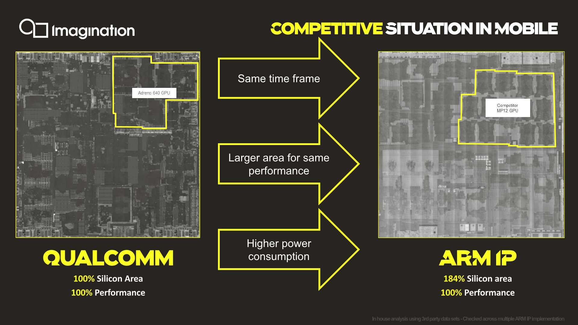
Starting off with a comparison between current generation Qualcomm GPU against an Arm GPU. Imagination didn’t specifically mention which designs we’re talking about here, but we do clearly see from the die shots that the SoCs being compared are the Snapdragon 855 and the Exynos 9820.
Here Imagination describes that for a similar performance level, Arm’s Mali GPUs are using ~184% the silicon area compared to Qualcomm’s Adreno implementation.
I do have some doubts about the validity of the comparison being made here, as these SoCs were not made on the same process node – Qualcomm's design is built on TSMC's denser 7nm process, while Samsung's Exynos uses their larger 8nm process. With that in mind, we take the metrics presented with a huge grain of salt as Imagination does say the figures are based on analysis of multiple Arm IP implementations rather than a single data-point.
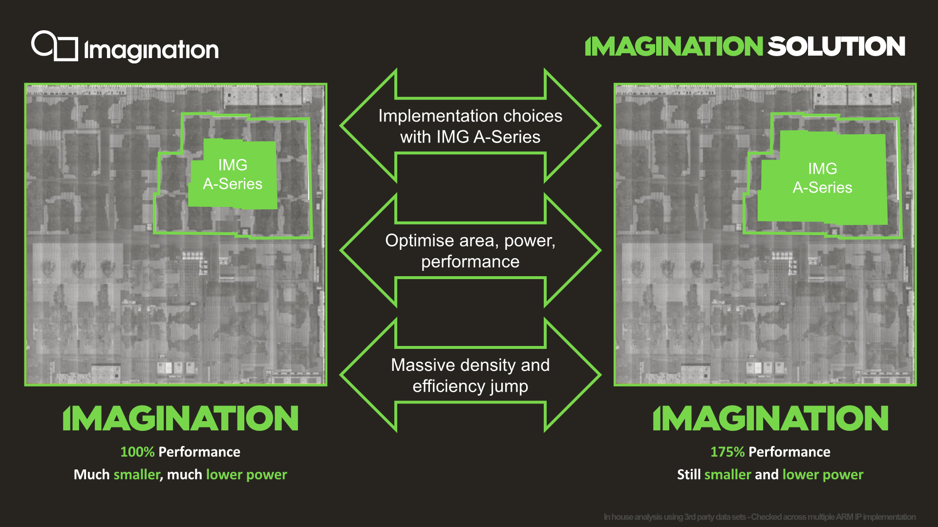
Projecting the A-Series against a current Mali-G76 implementation, targeting a performance level equivalent to current generation flagship implementations (~100fps in Manhattan 3.0), an A-Series GPU would achieve a significantly smaller GPU implementation requiring much less die area. The comparison implementation here would be an AXT-16-512 implementation running at slightly lower than nominal clock and voltage (in order to match the performance).
If a customer were to choose to use more die area to go wider and slower in clock (more efficient), while still maintaining an estimated area that would be smaller than a Mali GPU, it would roughly achieve a 75% performance advantage. The comparison here would be an AXT-32-1024 running quite far below nominal, giving it a large power efficiency advantage.
Of course, Imagination’s comparison here were made against the current generation Qualcomm and Arm GPUs, which aren't what it'll actually be competing against. Instead, by the time A-series SoCs ship, it will be competing against the next-generation Adreno as well as Mali-G77. We know Arm’s promised goals for the G77 and the improvements in performance per mm² and performance perf/W is around 1.2-1.4x, which we could generalize to 1.3x. Samsung’s upcoming Exynos 990 only promises a 20% performance increase, which is slightly below this projection. On the Qualcomm side and the upcoming Adreno generation, we’ll have to wait a few more days to be able to talk about details, but generally we expect improvements in the same ballpark.
Fortunately for Imagination, the projected PPA figures and advantages for the A-Series are high enough that they would still be notably ahead of both Qualcomm and Arm’s upcoming next generation GPUs, keeping a comfortable lead in either GPU area, or performance, depending on the configuration.
So far everything looks quite splendid – what remains to be seen if Imagination and their licensees are able to deliver on the projected figures.


143 Comments
View All Comments
mode_13h - Monday, December 9, 2019 - link
Nah, not in GPU parlance. Nvidia has long talked about each element of a SIMD as a thread. What CPU folks would call a "thread", Nvidia calls a "warp" and AMD calls a "wave". Not sure what Imagination calls it.ballsystemlord - Friday, December 20, 2019 - link
Grammar error:"...with for example each HyperLane having being able to be configured with its own virtual memory space..."
Excess words, try:
"...with for example each HyperLane having to be configured with its own virtual memory space..."
Fataliity - Saturday, December 28, 2019 - link
I bet you this GPU IS the Intel one, and Furian is the Ice Lake one. 64EU's at 1TFLOP = Ice Lake, 1GHz. Furian is 1/2 the speed of the A series.Intel's GPU is Xe. thisi s A - XE, XT, XM
But the base of 1/16 is called..... XE.
Add to that this
https://news.synopsys.com/2016-03-31-Intel-Custom-...
"certified on Intel 10nm PowerVR GT7200"
Who's buying this on Intel's process, and why is it ceritifed on IMGtech's GPU, if its not their integrated graphics under a different name?