Intel's new Atom Microarchitecture: The Tremont Core in Lakefield
by Dr. Ian Cutress on October 24, 2019 1:30 PM ESTTremont: A Wider Front End and Caches
For users that have been following our analysis of the Core microarchitecture, it has been hard not to notice that Intel’s design for that family has been, among other things, to continually go wider and wider. This means more instructions in flight, larger caches, bigger buffers, bigger TLBs, more execution ports, and support for more instructions. Going wider isn’t the only thing: the microarchitecture also has to be clever, trying to maximise utilisation, as going wider does nothing for a simple stream of commands.

With Atom, going wider is a key part of the design for Tremont, but Intel has taken a couple of fundamentally different steps to manage exactly what is going on.
A Key Uplift: Fetch and Predict
Another major jump for the Atom microarchitecture are the prefetchers and branch predictors. Intel states that rather than iterate the design from Goldmont Plus, they have transplanted a large part of the prefetchers and branch predictors from the Core design on Sunny Cove. The design isn’t identical according to Intel, due to die area and power concerns, but Intel states that the principles are similar and elements like branch prediction history tables are ‘of the same order’ as the Core design.

Intel states that there is no penalty for an L1 prediction, and that the L2 prediction penalty is smaller than previous generations.
A Key Differentiator: Decode Engines
On the face of it, we have a 6-wide decode engine pared with a 4-wide allocation/dispatch engine. This is, on paper, very odd: normally we would expect the decode and dispatch to be equal in width, or at least be able to dispatch more than can be decoded in order to ensure that the re-order buffer doesn’t overflow. With the latest Core microarchitecture, called Sunny Cove, we have a 4-to-6 wide decode that also supports a micro-op cache, which all leads into a large reorder buffer and a 10-wide dispatch to the back-end. Tremont is, by contrast, has the opposite ratio.
Saying that this is a 6-wide decode engine is actually slightly incorrect. What Intel has done here is split the decode into dual 3-wide engines instead.
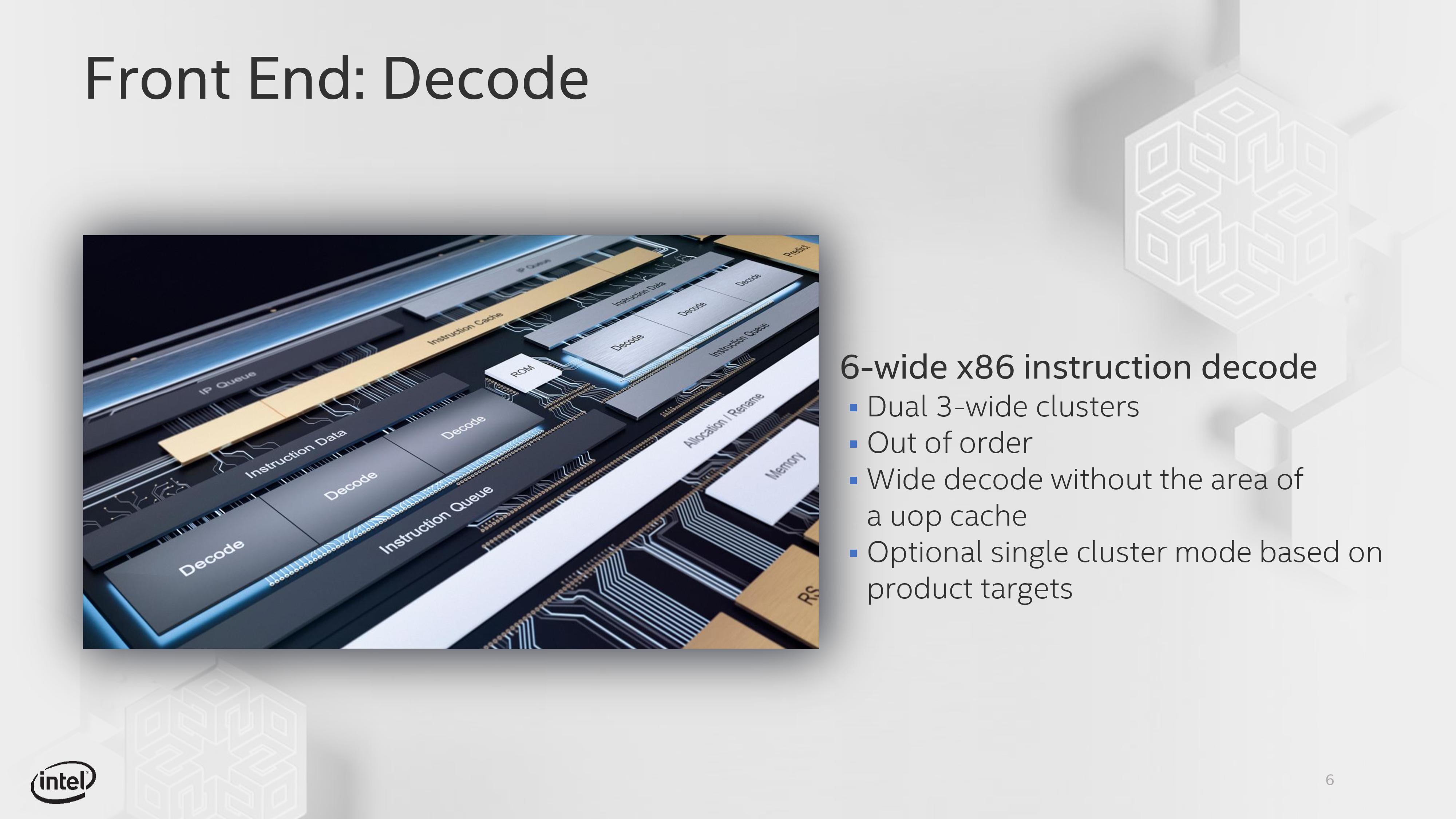
Each decode engine, when dealing with different branch predictions, can take a separate instruction stream. This allows for a higher average utilization across both of the 3-wide decode engines compared to a single 6-wide engine, but when a branch isn’t present it means that one of the decode engines can be clock gated to save power. For a single instruction stream, the Tremont design is actually only 3-wide decode, with a 4-wide dispatch.
(Technically Intel states that, through microcode, they can change the decode engines to act as a single 6-wide implementation rather than dual 3-wide engines. This won’t be configurable to the OEM, but based on demand Intel may make specific products for customers that request it.)
So just to clarify, Tremont does not have a micro-op cache. When discussing with Intel about the benefits of this dual decode engine design compared to having a micro-op cache, Intel stated that a micro-op cache can help utilize a wide-decode design better, but with a smaller per-engine decode size, they were able to see a performance uplift as well as save die area by using this dual-engine design. Intel declined to comment which one was better, but we were told that given the die size, power envelope of Atom, and the typical instruction flow of an Atom core, this design yielded the better combination of performance, power, and area.
Another improvement for Intel after the decode engines is the re-order buffer. Intel states that it can support 208 instructions, compared to 78 in Goldmont and 95 in Goldmont Plus, which is a sizeable uplift. Intel did not specify if Tremont has the ability to fuse instructions into micro-ops for the ROB (Goldmont did not), however there is a near 1:1 parity of instructions to micro-ops we were told.
Caches
Intel has also increased the size of its L1 data cache. The L1 instruction cache says at 32 KiB/core with 8-way associativity, but ever since the 22nm era, Intel has kept a 24 KiB/core L1 data cache on its Atom design. With Tremont, both the L1-I and L1-D are now a 32 KiB/core design with 8-way associativity. Intel states that its L1 data cache here has a 3-cycle latency, compared to Skylake which has a 32 KiB L1D at a 4-cycle latency, or Sunny Cove which has a 48 KiB L1D at a 5-cycle latency.
| Intel Caches | ||||||
| AnandTech | Tremont | Goldmont+ | Goldmont | Sunny Cove | Skylake | |
| Process | 10+ | 14 | 14 | 10+ | 14++ | |
| Decode | 2x3-wide | 3-wide | 3-wide | 4-6 wide | 4-5 wide | |
| Allocate | 4-wide | 4-wide | 3-wide | 10-wide | 8-wide | |
| L1 Instruction | 32 KiB/Core 8-way |
32 KiB/Core 8-way |
32 KiB/Core 8-way |
32 KiB/Core 8-way |
32 KiB/Core 8-way |
|
| L1 Data | 32 KiB/Core 8-way |
24 KiB/Core 6-way |
24 KiB/Core 6-way |
48 KiB/Core 12-way |
32 KiB/Core 8-way |
|
| L1 Latency | 3-cycle | 3-cycle | 3-cycle | 5-cycle | 4-cycle | |
| L2 Cache | 1.5-4.5 MiB Per Module 12-18 way |
1.0 MiB Per Core 16-way |
0.5-1.0 MiB Per Core 16-way |
512 KiB Per Core 8-way |
256 KiB Per Core 4-way |
|
| L2 Latency | 17-cycle | 19-cycle | 17-cycle | 13-cycle | 12 cycle | |
For the L2 cache, for most Atom cores in the past, this has essentially been a last-level cache split across all cores in a ‘module’. Depending on the generation will depend on the size of the module: for 22nm Silvermont, we saw an L2 cache of 512 KiB/core, which was increased with Goldmont up to 1.0 MB/core. With Tremont, Intel has specified that L2 will vary depending on the product, from 1.5 MiB to 4.5 MiB per module. A module for Tremont will be anything up to four cores, so we could see designs with a single core featuring 4.5 MiB of L2 cache, or a quad-core design with 1.5 MiB of L2. Within a module, all cores have access to the cache, however a core will not have access to the L2 in a different module. The L2 can be set through microcode as an inclusive or a non-inclusive cache.
Intel states that the L2 cache has an average 17-cycle latency, and the associativity will be a function of the size: 1.5 MB will be a 12-way design, while 4.5 MB will be an 18-way design. (We therefore assume that a 3.0 MB L2 will be 15-way.)
Tremont also adds support for a global L3 cache across modules. Both the L2 and L3 cache support QoS arrangements, allowing for data prioritization and memory bandwidth enforcement for specific threads or virtual machines. This is a technology that Intel introduced with Broadwell Xeons to help avoid ‘noisy neighbor’ environments in data centers.


101 Comments
View All Comments
Namisecond - Friday, November 1, 2019 - link
Which will be far more important for devices that run Windows.petr.koc - Friday, October 25, 2019 - link
"the enterprise side has been dealing with a clock degradation issue that ultimately leaves Atom systems built on C2000 processors unable to boot,"This is unfortunately not precise as all Atom Bay Trail processors (desktop, mobile, server) including 14nm successors manufactured up to approximately 2018 are affected with LPC circuitry degradation issue that will kill them in the end:
https://en.wikipedia.org/wiki/Silvermont#Erratum
https://en.wikipedia.org/wiki/Goldmont#Erratum
29a - Friday, October 25, 2019 - link
Ugh, I just look at your links and I have a NAS box with a J1900. I wonder what can be done to replace it?MASSAMKULABOX - Thursday, October 31, 2019 - link
Yeah, I'm amazed this didnt byte Intel in the Ass much harder, AFAIK synology and cisco were both victims and I'm sure many others. So, start by making well-tested, reliable products.. and no harm in boosting up the GFX side of things (x2 X3?). Give us desktop systems @10w and lowerBigos - Friday, October 25, 2019 - link
> (We therefore assume that a 3.0 MB L2 will be 15-way.)That is very unlikely. 3.0MB (which is 3 * 1024 * 1024) is not divisible by 15. I'm sure the 3MB L2$ will be 12-way associative.
1.5MB = 12 * 128kB
3.0MB = 12 * 256kB
4.5MB = 18 * 256kB
AntonErtl - Friday, October 25, 2019 - link
It's clear that they drop products with low-$/area when they do not have enough capacity, but AFAIK that's not the case at the moment for 10nm; on the contrary, they have 10nm capacity and not much demand for Ice Lake (because they cannot get the clock rates and efficiency competetive with the 14nm Skylake derivatives). So building Tremont-based successors for Gemini Lake (where performance is not as critical) would be a way for them to get more revenue out of their 10nm production line(s?); of course they have to design that first, and they may have failed to do so, expecting Ice Lake production to be in full swing by now.Concerning sucking performance, here are some numbers for our LaTeX benchmark http://www.complang.tuwien.ac.at/franz/latex-bench...
2.368 Intel Atom 330, 1.6GHz, 512K L2 Zotac ION A
1.052 Celeron J1900 (Silvermont) 2416MHz (Shuttle XS35V4)
0.712 Celeron J3455 (Goldmont) 2300MHz, ASRock J3455-ITX
0.540 Celeron J4105 (Goldmont+) 2500MHz
0.200 Core i7-6700K (Skylake), 4200MHz
Skylake has about a factor 1.6 better IPC than Goldmont+, and allows higher clock rates (at higher power consumption), resulting in significantly better overall performance, but whether that makes the Goldmont+ suck depends on the application.
29a - Friday, October 25, 2019 - link
Decoding video, that's what the other two Atoms I've owned sucked at.PeachNCream - Friday, October 25, 2019 - link
You keep thrashing at that, but other people that have dissimilar experiences have supported claims that run contrary to your statements. What model Atoms and under what conditions haev you had this problem? This isn't an issue for anyone else and, frankly, watching video isn't the only thing a computer does so that complaint may have no impact on the wider range of use cases beyond watching YouTube and Netflix.Jorgp2 - Friday, October 25, 2019 - link
He probably has an in order atom.Pretty much all out of order atoms have hardware decoding acceleration
GreenReaper - Saturday, October 26, 2019 - link
Or, he's trying to decode a video that isn't supported by the hardware. Like 10-bit anything until very recent. In fairness my Bobcat cores struggle with 60FPS anything, and plain Full HD MP4 decode also bogs down if you add anything but the most minimal of shader filters. But they're from ~2011.