Intel's new Atom Microarchitecture: The Tremont Core in Lakefield
by Dr. Ian Cutress on October 24, 2019 1:30 PM ESTA Wider Back End
Moving beyond the micro-op queue, Tremont has an 8 execution ports, filled from 7 reservation stations.
The only two ports using a combined reservation station are the address generator units (AGUs) - this is in stark contrast to the Core design, which in Sunny Cove uses a unified reservation for all integer and floating point calculations and three for the AGUs. The reason that Tremont uses a unified reservation station for the two AGUs, also backed by extra memory for queued micro-ops, is in order to supply both AGUs with either 2x 16-byte stores, 2x 16-byte loads, or one of each. Intel clearly expects the AGUs on Tremont to be fairly active compared to other execution ports.

On the integer side, aside from the two AGUs, Tremont has 3 ALUs, a jump port, and a store data port. Each ALU supports different functions, with one enabling shift functions and another for multiplication and division. Compared to core, these ALUs are extremely lightweight, and Intel hasn’t gone into specifics here.
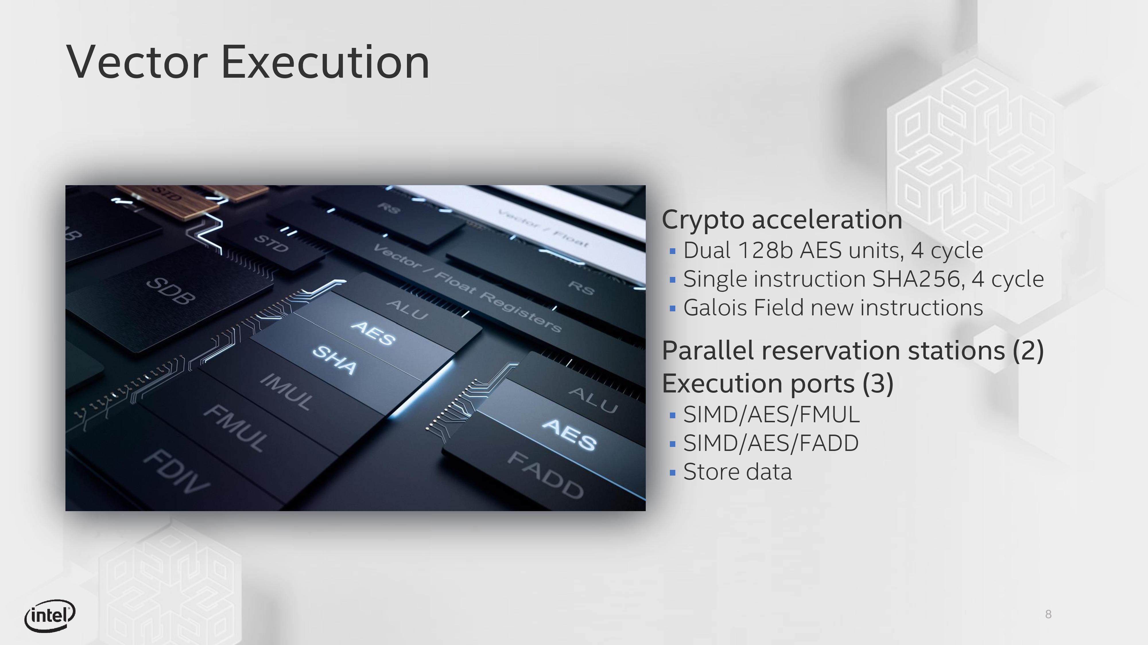
On the floating point side, we are a little bit more varied – the three ports are split between two ALUs and a store port. The two ALUs have one focused on fused additions (FADD), while the other focuses on fused multiplication and division (FMUL). Both ALUs support 128-bit SIMD and 128-bit AES instructions with a 4-cycle latency, as well as single instruction SHA256 at 4-cycles. There is no 256-bit vector support here. In order to help with certain calculations, GFNI instruction support is included.
There is also a larger 1024-entry L2 TLB, supporting 1024x 4K entries, 32x 2M entries, or 8x 1G entries. This is an upgrade from the 512-entry L2 TLB in Goldmont.
New Instructions
As with any generation, Intel adds new supported instructions to either accelerate common calculations that would traditionally require lots of instructions or to add new functionality. Tremont is no different.
| TITLE | |||||
| AnandTech | Tremont | Goldmont Plus |
Goldmont | Airmont | Silvermont |
| Process | 10+ | 14 | 14 | 14 | 22 |
| Release Year | 2019 | 2017 | 2016 | 2015 | 2013 |
| New Instructions | CLWB GFNI ENCLV CLDEMOTE MOVDIR* TPAUSE UMONITOR UWAIT |
SGX1 UMIP PTWRITE RDPID |
RDSEED SMAP MPX XSAVEC XSAVES CLFLUSHOPT SHA |
SSE4.1 SSE4.2 MOVBE CRC32 POPCNT CLMUL AES RDRAND PREFETCHW |
|
(When asked what other new instructions are supported, Intel stated to look at the published documents about future instructions. When it was pointed out that those documents weren’t exactly clear and that in the past Intel hasn’t spoken about future designs, we were not afforded additional comments.)
When we get hold of a Tremont device, we’ll do a full instruction breakdown.


101 Comments
View All Comments
mode_13h - Saturday, October 26, 2019 - link
Yes, fadd is simply floating-point add. Same for fmul.What makes FMA "fused" is that the product isn't truncated before the accumulate, resulting in higher precision. So, what's "fused" is the multiplication and accumulation.
Fused-add or fused-multiply makes no sense - they each only do one thing, so what would you even be fusing?
The Hardcard - Thursday, October 24, 2019 - link
when I squint at the power/performance graph, I don’t see much of a power savings for Tremont. If that is 1.5 for Sunny, it looks like Tremont is will be more like 1 watt rather than 200mW. is it my eyes or are they being loose with the graph. also, it looks like performance drops much faster than power.Lakefield seems like it should be 2+4 rather than 1+4. it will be interesting to see how it compares to the 8cx for performance and battery life.
Santoval - Thursday, October 24, 2019 - link
In the graph Sunny Cove goes down to 12 - 13% "relative power" while Tremont reaches around 4 - 5%. So, if we assume a lowest of 13% relative power for Sunny Cove at 1.5W and a lowest of 4% for Tremont, this would suggest that Sunny Cove at its lowest power/frequency consumes 3.25 (13/4) times more power than Tremont at its lowest power/frequency.If that's indeed the case, and that graph is accurate, then Tremont consumes ~0.45 watts (1.5W / 3.25) at its lowest power, not 1 watt. However if that graph is only slightly inaccurate Tremont might really go down to 200mW operation mode. For instance if Sunny Cove's relative power was meant to terminate at 20% and Tremont's at 3% then their difference in power consumption at the lowest power mode is (20/3) 6.67 times, thus Tremont would go down to ~220mW.
The Hardcard - Thursday, October 24, 2019 - link
interesting, we both put Sunny at 12 percent. But my eyes put Tremont at 8 percent, which is how I got one watt. It just looks much closer to the 10 than the one. But, I assume Microsoft got figures that made sense to them so maybe you’re right.name99 - Friday, October 25, 2019 - link
We have to look at why this product exists. To me it looks like IBM's 8-way threading, ie a product of the decadent stage of CPU design, when the primary impulse becomes to game the markets rather than to optimize engineering metrics.Look at the performance/energy curve. There is SO MUCH overlap with Core. That makes little sense for a big.LITTLE type system -- if the primary goal is low power, you optimize the one core for low power, the other for performance, and make little effort to extend the low power performance beyond the lowest the high power core goes. (You want a small amount of overlap for hysteresis but not much more.) If you look at Apple's cores (which I know best) this is clear; the small cores max at about 30% of the performance of the large cores, and the large cores can clock down to about 1/3 maximum frequency.
But what if your goal is NOT primarily energy saving? The Tremont presentation talks a whole lot about performance, little (nothing that I saw) about where they saved energy and how much. What if your goal is to create a "reasonably powerful" lower end core, to at least good enough match current ARM AND to be able to expand your provision of multi-core (for PCs) and many-core (for laptops) without having to give up those nice juicy Core profits?...
Clearly you can think of Tremont as an A75 equivalent, to be sold to designs thinking of jumping ship at that performance level. But you can also view it as Intel's way of providing low-end laptops/desktops with 5 (or 6? who knows what the SMT situation of the large core is) threads without having to drop the prices on i5s. Likewise a way to compete with those 48 and 64-core lightweight ARMs (ThunderX, Cavium and suchlike) while again not having to drop the price of the large Xeons.
In this light, the omission of decent AVX is not a bug, it's a feature; it's one more reason that these are low class cores meant for peasants, while decent people should continue to pay for Cores.
On financial grounds, this may make sense, and Intels' plan is presumably to add AVX-512 when SVE becomes too common too ignore (but not until then...)
On strategic grounds does it make sense? Hmm.
- It may just prevent even more people from ever bothering to design, compile, and optimize for AVX. Maybe likewise for persistent memory? (That support seems pretty fragmented, and I'm sure Tremont won't help.)
- Even Intel isn't so large that they can keep creating substantially improved new designs every year (something that's become very clear over the past few years).
This particular fork seems to be one that doesn't allow for that much learning across the two teams (and may even lead to deliberate crippling if the Tremont direction gets "too" good).
Of course other design houses are even more opaque than Intel (I don't think we have any idea how much cross-learning there is between the ARM big and little core teams. Apple certainly APPEARS to have very good cross-learning [both the lock-step feature support and the very low performance overlap as minor pieces of evidence] but who can be sure?)
But they seem to have a better aligned set of incentives to keep everyone happy and in sync. (Team A goes for performance at this power level, team B for performance up to X and no further and this lower power level.)
Whereas Intel seems to be in the difficult situation (that VERY WIDE performance overlap range between the two cores) of "yeah, keep making it faster, but not too fast --- you'll know when you're too fast because we'll crush your spirit at that point..."
Anyway, lots of rambling here, but I think the key insight is to NOT see this as an ENERGY big.LITTLE play, regardless of what Intel says, but as a way to provide more cores at the low-end without hurting Core prices. (Of course there is still that pesky damn AMD forcing high-end Xeon prices to halve... Well, one battle at a time.)
Namisecond - Friday, November 1, 2019 - link
8cx will probably beat Lakefield in terms of efficiency, but Lakefield has native x86 and probably better perceived performance.azfacea - Thursday, October 24, 2019 - link
wrong title. this aint new. its pentium 4 shrink/rebrandJorgp2 - Thursday, October 24, 2019 - link
Lol, norozquilla - Thursday, October 24, 2019 - link
I love my J5005 (Gemini Lake) as an HTPC, and I lent it to a relative for a while after his AMD A10-7860K (Piledriver, meh...) failed, he felt it worked around the same, and faster on videos...Which is why I love this CPU, it is fanless and stays at around ~8W and plays back 10bit 4K content in my living room TV without any issues. I also added a CNVI 802.11ac module, it performs great.
Hopefully this Tremont Core will provide something like that, but I will upgrade until there is AV1 hardware decoding. With which GPU will it be paired, a Gen11 something? I think AV1 is still a bit down the road with x86, ARM already has a couple of proposals.
For day to day office and HTPC duties, I haven't found a better alternative (maybe RPi4 in this segment?), I'm also waiting to see the Ryzen embedded alternatives for home use, so far only expensive industrial-ish options.
GreenReaper - Thursday, October 24, 2019 - link
Usually the video block is shared across all segments, so if the APU form of Navi picks up AV1 support, chances are it'll be available. Might be a while until truly low-end APUs are available, though.