Intel's new Atom Microarchitecture: The Tremont Core in Lakefield
by Dr. Ian Cutress on October 24, 2019 1:30 PM ESTTremont: A Wider Front End and Caches
For users that have been following our analysis of the Core microarchitecture, it has been hard not to notice that Intel’s design for that family has been, among other things, to continually go wider and wider. This means more instructions in flight, larger caches, bigger buffers, bigger TLBs, more execution ports, and support for more instructions. Going wider isn’t the only thing: the microarchitecture also has to be clever, trying to maximise utilisation, as going wider does nothing for a simple stream of commands.

With Atom, going wider is a key part of the design for Tremont, but Intel has taken a couple of fundamentally different steps to manage exactly what is going on.
A Key Uplift: Fetch and Predict
Another major jump for the Atom microarchitecture are the prefetchers and branch predictors. Intel states that rather than iterate the design from Goldmont Plus, they have transplanted a large part of the prefetchers and branch predictors from the Core design on Sunny Cove. The design isn’t identical according to Intel, due to die area and power concerns, but Intel states that the principles are similar and elements like branch prediction history tables are ‘of the same order’ as the Core design.

Intel states that there is no penalty for an L1 prediction, and that the L2 prediction penalty is smaller than previous generations.
A Key Differentiator: Decode Engines
On the face of it, we have a 6-wide decode engine pared with a 4-wide allocation/dispatch engine. This is, on paper, very odd: normally we would expect the decode and dispatch to be equal in width, or at least be able to dispatch more than can be decoded in order to ensure that the re-order buffer doesn’t overflow. With the latest Core microarchitecture, called Sunny Cove, we have a 4-to-6 wide decode that also supports a micro-op cache, which all leads into a large reorder buffer and a 10-wide dispatch to the back-end. Tremont is, by contrast, has the opposite ratio.
Saying that this is a 6-wide decode engine is actually slightly incorrect. What Intel has done here is split the decode into dual 3-wide engines instead.
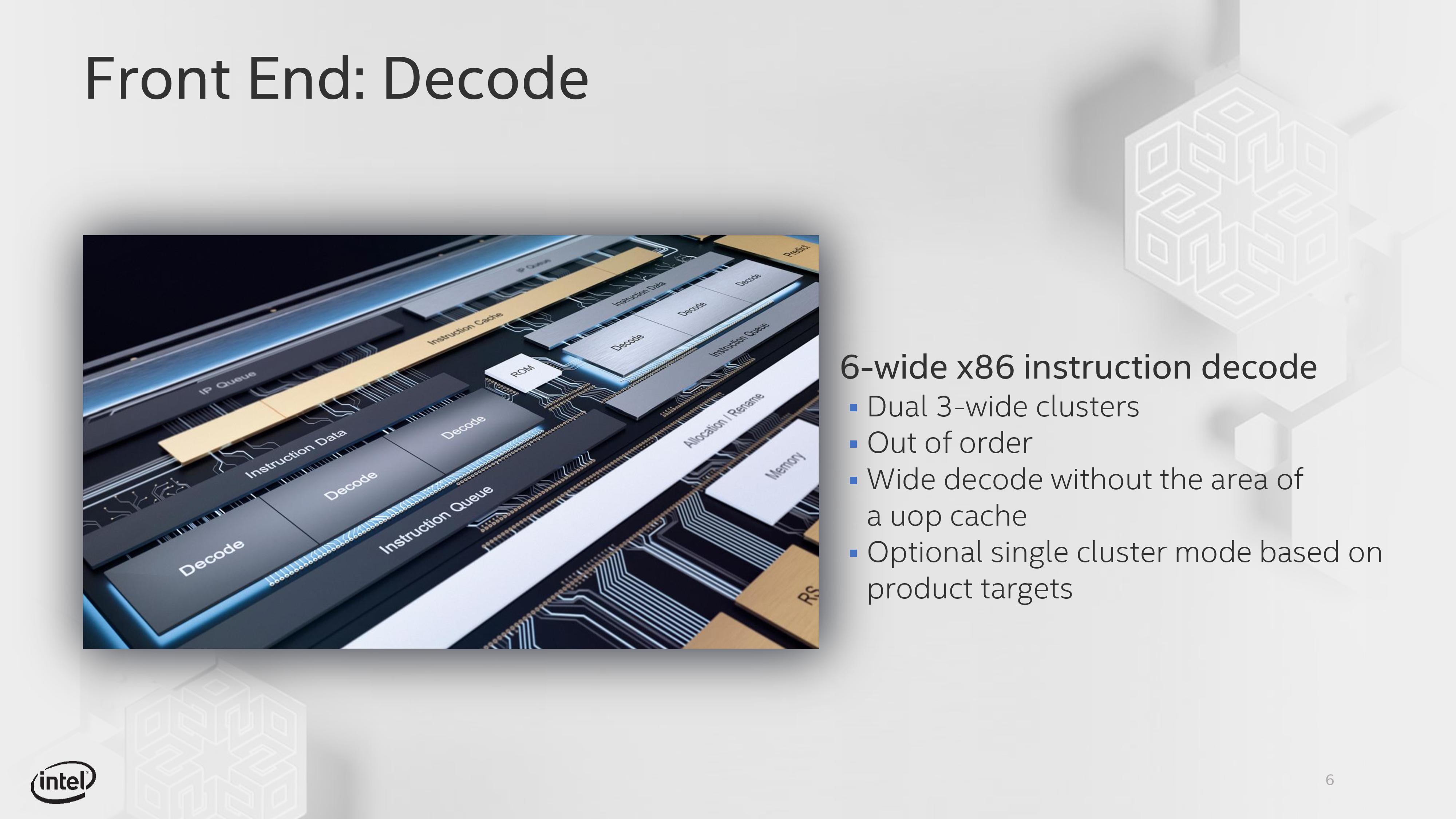
Each decode engine, when dealing with different branch predictions, can take a separate instruction stream. This allows for a higher average utilization across both of the 3-wide decode engines compared to a single 6-wide engine, but when a branch isn’t present it means that one of the decode engines can be clock gated to save power. For a single instruction stream, the Tremont design is actually only 3-wide decode, with a 4-wide dispatch.
(Technically Intel states that, through microcode, they can change the decode engines to act as a single 6-wide implementation rather than dual 3-wide engines. This won’t be configurable to the OEM, but based on demand Intel may make specific products for customers that request it.)
So just to clarify, Tremont does not have a micro-op cache. When discussing with Intel about the benefits of this dual decode engine design compared to having a micro-op cache, Intel stated that a micro-op cache can help utilize a wide-decode design better, but with a smaller per-engine decode size, they were able to see a performance uplift as well as save die area by using this dual-engine design. Intel declined to comment which one was better, but we were told that given the die size, power envelope of Atom, and the typical instruction flow of an Atom core, this design yielded the better combination of performance, power, and area.
Another improvement for Intel after the decode engines is the re-order buffer. Intel states that it can support 208 instructions, compared to 78 in Goldmont and 95 in Goldmont Plus, which is a sizeable uplift. Intel did not specify if Tremont has the ability to fuse instructions into micro-ops for the ROB (Goldmont did not), however there is a near 1:1 parity of instructions to micro-ops we were told.
Caches
Intel has also increased the size of its L1 data cache. The L1 instruction cache says at 32 KiB/core with 8-way associativity, but ever since the 22nm era, Intel has kept a 24 KiB/core L1 data cache on its Atom design. With Tremont, both the L1-I and L1-D are now a 32 KiB/core design with 8-way associativity. Intel states that its L1 data cache here has a 3-cycle latency, compared to Skylake which has a 32 KiB L1D at a 4-cycle latency, or Sunny Cove which has a 48 KiB L1D at a 5-cycle latency.
| Intel Caches | ||||||
| AnandTech | Tremont | Goldmont+ | Goldmont | Sunny Cove | Skylake | |
| Process | 10+ | 14 | 14 | 10+ | 14++ | |
| Decode | 2x3-wide | 3-wide | 3-wide | 4-6 wide | 4-5 wide | |
| Allocate | 4-wide | 4-wide | 3-wide | 10-wide | 8-wide | |
| L1 Instruction | 32 KiB/Core 8-way |
32 KiB/Core 8-way |
32 KiB/Core 8-way |
32 KiB/Core 8-way |
32 KiB/Core 8-way |
|
| L1 Data | 32 KiB/Core 8-way |
24 KiB/Core 6-way |
24 KiB/Core 6-way |
48 KiB/Core 12-way |
32 KiB/Core 8-way |
|
| L1 Latency | 3-cycle | 3-cycle | 3-cycle | 5-cycle | 4-cycle | |
| L2 Cache | 1.5-4.5 MiB Per Module 12-18 way |
1.0 MiB Per Core 16-way |
0.5-1.0 MiB Per Core 16-way |
512 KiB Per Core 8-way |
256 KiB Per Core 4-way |
|
| L2 Latency | 17-cycle | 19-cycle | 17-cycle | 13-cycle | 12 cycle | |
For the L2 cache, for most Atom cores in the past, this has essentially been a last-level cache split across all cores in a ‘module’. Depending on the generation will depend on the size of the module: for 22nm Silvermont, we saw an L2 cache of 512 KiB/core, which was increased with Goldmont up to 1.0 MB/core. With Tremont, Intel has specified that L2 will vary depending on the product, from 1.5 MiB to 4.5 MiB per module. A module for Tremont will be anything up to four cores, so we could see designs with a single core featuring 4.5 MiB of L2 cache, or a quad-core design with 1.5 MiB of L2. Within a module, all cores have access to the cache, however a core will not have access to the L2 in a different module. The L2 can be set through microcode as an inclusive or a non-inclusive cache.
Intel states that the L2 cache has an average 17-cycle latency, and the associativity will be a function of the size: 1.5 MB will be a 12-way design, while 4.5 MB will be an 18-way design. (We therefore assume that a 3.0 MB L2 will be 15-way.)
Tremont also adds support for a global L3 cache across modules. Both the L2 and L3 cache support QoS arrangements, allowing for data prioritization and memory bandwidth enforcement for specific threads or virtual machines. This is a technology that Intel introduced with Broadwell Xeons to help avoid ‘noisy neighbor’ environments in data centers.


101 Comments
View All Comments
eddman - Saturday, October 26, 2019 - link
MP4 is a container, not a codec.Alien959 - Friday, October 25, 2019 - link
I am reading this article on goldmont + powered laptop. While definitely is not a speedster, the hardware is perfectly usable for light tasks like internet browsing, text editing I even did some 1080p edits in premiere and some modeling in SketchUp pro. It handles the tasks fine. The rest of the hardware is a ssd and 8 gb of ddr4 ram. The main reason what makes the system usable is that the GPU is supported in both programs, and that alleviates the speed of weaker cores on the CPU side.Bigos - Friday, October 25, 2019 - link
> The two ALUs have one focused on fused additions (FADD), while the other focuses on fused multiplication and division (FMUL).Did you mean *float* instead of fused? The only thing that comes to my mind when you say "fused" is FMA: fused multiply-accumulate.
Also, in the "New Instructions" section the table is titled "TITLE", which sounds amusing but is probably a left-over.
mode_13h - Saturday, October 26, 2019 - link
Yeah, this was also mentioned above. You are correct, as I said in my reply to @ternnence.snakyjake - Friday, October 25, 2019 - link
If it works for HTPC, decodes HEVC efficiently, low power, low heat, fanless, then I'll buy it.Namisecond - Friday, November 1, 2019 - link
The current Goldmont+ chips already do all that.ksec - Saturday, October 26, 2019 - link
Not useful without pricing. In terms of absolute numbers in both Performance and power, ARM or POWER has readily available solutions.Elstar - Saturday, October 26, 2019 - link
The dual frontend decoders seem ideal for SMT performance. I'm surprised they don't have that option for those that want it.TomWomack - Sunday, October 27, 2019 - link
'1.5 MB will be a 12-way design, while 4.5 MB will be an 18-way design. (We therefore assume that a 3.0 MB L2 will be 15-way'1.5MB 12-way would be 12 256kb blocks; 4.5MB 18-way would be 18 512kb blocks; 3.0MB would be either 24-way with 256kb blocks or 12-way with 512kb blocks, almost certainly the latter
AshlayW - Sunday, October 27, 2019 - link
Intel's new SoC design with "low power" and "high power" cores, akin to the big.LITTLE from ARM, is actually pretty awesome. I'll give them credit where it's due, Sunny Cove, and Tremont are shaping up to be fantastic architectures - for low power mobile, an area where I'd love to see more super tiny low power x86 devices, as I have grown quite fond of my HP envy X360, even though it has the comparatively less efficient Raven Ridge silicon in it (2500U).It's just a shame they won't have anything interesting on the desktop. I'll tell you what, Intel. If you want my custom, get these ULP chips into something like a One mix Yoga 3, and I might even buy it. Now imagine playing Warframe, on the go, on a device I can slip in my pocket with a wireless Xbox Controller in the other one. Make it happen.