Examining Intel's Ice Lake Processors: Taking a Bite of the Sunny Cove Microarchitecture
by Dr. Ian Cutress on July 30, 2019 9:30 AM EST- Posted in
- CPUs
- Intel
- 10nm
- Microarchitecture
- Ice Lake
- Project Athena
- Sunny Cove
- Gen11
Wi-Fi 6: Implementing AX over AC*
In consumer products, Intel has been placing its new Wi-Fi initiative into every chipset it can find. We’ve seen CNVi-enabled solutions occur on the desktop and in the notebook space for almost two years now, with the goal to make high-performance and low-power Wi-Fi ubiquitous, and to push Intel’s wireless solutions everywhere. Ice Lake is where Intel enables Wi-Fi 6 in such a solution.
If you’ve never come across the term CNVi before, it is Intel’s proprietary interface link and controller which connects the logic parts of the wireless connection on the chipset to the antenna and radio frequency analog parts which are found on a different module. This allows Intel’s partners to use different antenna ‘RF’ modules depending on what it wants to support, such as single antenna designs, dual antenna designs, or higher bandwidth modes.
Because CNVi is a proprietary interface, Intel has no plans to license it, and therefore the only RF modules you can buy to support it come from Intel. Intel states that its CNVi solution enables the high frequency digital logic to be built on its 14nm process with the chipset, and the RF analog side can be built on 28nm UMC which is better for analog signals and performance than any of Intel’s currently available manufacturing processes. Overall Intel states that using an external RF chip in this fashion affords a 15% silicon package reduction and a 40% pin reduction.

CNVi RF modules can either be an M.2 module (2230 = 22mm x 30mm) or as a soldered module (1216), which respectively allows for modularity, or for decreasing z-height for thin and light designs. Intel also states that this method of supplying the Wi-Fi, as separate digital and analog silicon, allows Wi-Fi certification to be done at the module level, rather than at the system level, simplifying the process for its partners.
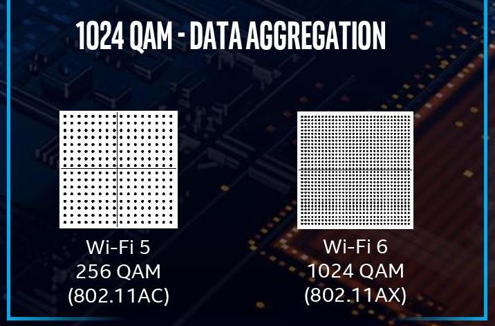
As an overarching technology, Wi-Fi 6 promises better bandwidth than standard Wi-Fi 5, as well as support for more devices on the same network. Technically this increased bandwidth comes down to data/time aggregation through the air as a benefit of OFDMA support, as well as 1024-QAM signaling design rather than 256-QAM signaling for increased throughput.

Wi-Fi 6 also has a lot of additional optional elements to the standard, which Intel believes will cause a good deal of confusion in the market. Naturally, Intel suggests that its partners that use a CNVi Wi-Fi 6 implementation also promote Wi-Fi 6 access points built on Intel’s platforms for simpler integration.
At this point in time, there are two main Wi-Fi 6 controllers: Intel’s AX200/AX201 2x2 CNVi module which uses the on-die enhancements, and Rivet Network’s AX1650 M.2 module which doesn’t use any of the on-die enhancements as it connects through a PCIe lane on the chipset. Technically both are built with the same silicon, as the companies are working together on the design, however Rivet is implementing its own acceleration techniques due to engines inside the hardware.
*The asterisk in the title of this page is because you still need external hardware in order to enable it, and to do it in the best way requires Intel-only hardware. You can use other vendor hardware, but you don’t need something special on the SoC to enable that.


107 Comments
View All Comments
repoman27 - Tuesday, July 30, 2019 - link
"It stands to reason then that the smaller package is for lower performance and low power options, despite being exactly the same silicon."I know the die floorplans are the same, but have Intel ever actually confirmed that U and Y (or H and S series for that matter) are the exact same silicon? Is it strictly binning and packaging that separates the platforms, or is there a slight tweak to the manufacturing process to target lower power / higher frequencies? Intel production roadmaps would seem to indicate this isn't just a binning situation, but I've never been entirely certain on that point.
And isn't Comet Lake-U 6+2 more likely to be 25 W, with Whiskey Lake-U 4+2 continuing to pull 15 W duty alongside Ice Lake-U 4+2?
CaedenV - Tuesday, July 30, 2019 - link
Those goals for Aethena are OK, but my old Dell XPS 12 with a carousel frame hit all of those except biometric, and wake from sleep in <1 sec... well, and the bezel... but that was due to the carousel design which I would LOVE to come back in a more modern form.Not saying these goals are bad... but if a 6 year old midrange laptop can hit almost all of them, then this isn't exactly aiming for something amazing.
AshlayW - Tuesday, July 30, 2019 - link
Quad core for 179 USD? What is this, 2015? No thanks.HStewart - Tuesday, July 30, 2019 - link
You do realize these are ultra-portable low power cpu's and not desktop chipsSamus - Tuesday, July 30, 2019 - link
Intel is a mess right now, the execution of this along with the naming scheme is ridiculous.shabby - Tuesday, July 30, 2019 - link
18% ipc gain and 20% clock lossPlace your bets how intel will spin this.
CHADBOGA - Tuesday, July 30, 2019 - link
I'm quite disappointed the issue of security mitigation in hardware was not addressed. o_OCityBlue - Saturday, August 3, 2019 - link
Disappointed, but not surprised.Security (and by inference the performance overhead required to implement proper security) is not important according to Anandtech/Ian Cutress. Which is obvious nonsense, so the only logical conclusion is that Anandtech are now a thoroughly biased outfit incapable of any critical reporting, which is quite sad particularly as it means all their articles (particularly when they relate to Intel) have to be read with a very heavy dose of cynicism.
eek2121 - Wednesday, July 31, 2019 - link
That picture of you biting a wafer is priceless.Santoval - Wednesday, July 31, 2019 - link
If Ice Lake-U has a ~3.5% higher single core performance (and, assuming the "multi-core overhead" is the same, multi-core performance as well) than Whiskey Lake-U despite having a 20% lower single core boost clock, then Sunny Cove must be an extremely impressive μarch. Or, er, that might not actually be the case : Ice Lake-U has a 18% higher IPC than the *original* Skylake of 2015, not Whiskey Lake. While Whiskey Lake is basically the same design it must have a somewhat higher IPC due to its much more mature process node and other optimizations.Let's be conservative and assume that Ice Lake-U (more specifically Sunny Cove) has a nice round 15% higher IPC than Whiskey Lake-U, with both at 15W. In that case, at a 20% lower boost clock Ice Lake-U should have a 5% lower performance than Whiskey Lake-U. Where is that +3.5% performance derived from then?
Even if we assumed that Ice Lake-U 18% IPC edge is over Whiskey Lake-U (highly unlikely, otherwise Intel would not have dug out the original Skylake from its computing grave) that would still translate to Ice Lake-U having a 1.5% lower single core performance than Whiskey Lake-U, rather than being 3.5% faster than it.
Maybe, just maybe, this is why Intel used just a single synthetic benchmark (surely compiled with aggressive flags and optimized for Intel CPUs) for that graph and avoided to disclose other synthetic benchmarks and real world use benchmarks? Is this also why they avoided to talk about CPU performance of Ice Lake in their Computex presentation, and instead focused on iGPU, Wifi and AI performance?
Based on the disclosed clocks and the "disclosed" (in obfuscated form) IPC of Ice Lake-U I just cannot see it being in any way faster than Whiskey Lake-U. It will probably also have worse power efficiency, since it has the same or higher TDP range at a much lower clock.