Examining Intel's Ice Lake Processors: Taking a Bite of the Sunny Cove Microarchitecture
by Dr. Ian Cutress on July 30, 2019 9:30 AM EST- Posted in
- CPUs
- Intel
- 10nm
- Microarchitecture
- Ice Lake
- Project Athena
- Sunny Cove
- Gen11
Wi-Fi 6: Implementing AX over AC*
In consumer products, Intel has been placing its new Wi-Fi initiative into every chipset it can find. We’ve seen CNVi-enabled solutions occur on the desktop and in the notebook space for almost two years now, with the goal to make high-performance and low-power Wi-Fi ubiquitous, and to push Intel’s wireless solutions everywhere. Ice Lake is where Intel enables Wi-Fi 6 in such a solution.
If you’ve never come across the term CNVi before, it is Intel’s proprietary interface link and controller which connects the logic parts of the wireless connection on the chipset to the antenna and radio frequency analog parts which are found on a different module. This allows Intel’s partners to use different antenna ‘RF’ modules depending on what it wants to support, such as single antenna designs, dual antenna designs, or higher bandwidth modes.
Because CNVi is a proprietary interface, Intel has no plans to license it, and therefore the only RF modules you can buy to support it come from Intel. Intel states that its CNVi solution enables the high frequency digital logic to be built on its 14nm process with the chipset, and the RF analog side can be built on 28nm UMC which is better for analog signals and performance than any of Intel’s currently available manufacturing processes. Overall Intel states that using an external RF chip in this fashion affords a 15% silicon package reduction and a 40% pin reduction.

CNVi RF modules can either be an M.2 module (2230 = 22mm x 30mm) or as a soldered module (1216), which respectively allows for modularity, or for decreasing z-height for thin and light designs. Intel also states that this method of supplying the Wi-Fi, as separate digital and analog silicon, allows Wi-Fi certification to be done at the module level, rather than at the system level, simplifying the process for its partners.
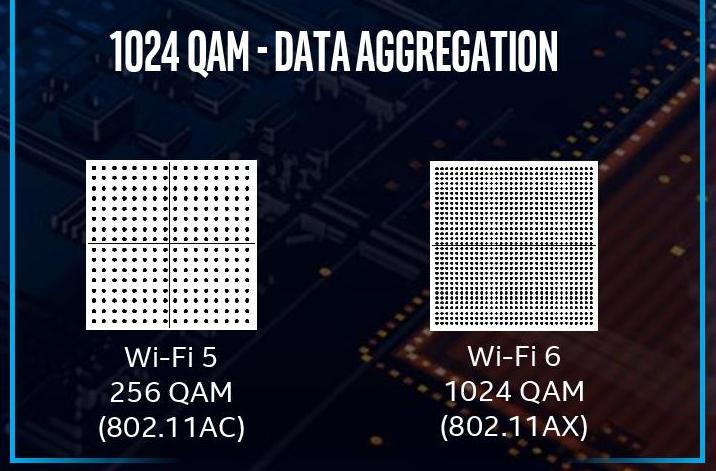
As an overarching technology, Wi-Fi 6 promises better bandwidth than standard Wi-Fi 5, as well as support for more devices on the same network. Technically this increased bandwidth comes down to data/time aggregation through the air as a benefit of OFDMA support, as well as 1024-QAM signaling design rather than 256-QAM signaling for increased throughput.

Wi-Fi 6 also has a lot of additional optional elements to the standard, which Intel believes will cause a good deal of confusion in the market. Naturally, Intel suggests that its partners that use a CNVi Wi-Fi 6 implementation also promote Wi-Fi 6 access points built on Intel’s platforms for simpler integration.
At this point in time, there are two main Wi-Fi 6 controllers: Intel’s AX200/AX201 2x2 CNVi module which uses the on-die enhancements, and Rivet Network’s AX1650 M.2 module which doesn’t use any of the on-die enhancements as it connects through a PCIe lane on the chipset. Technically both are built with the same silicon, as the companies are working together on the design, however Rivet is implementing its own acceleration techniques due to engines inside the hardware.
*The asterisk in the title of this page is because you still need external hardware in order to enable it, and to do it in the best way requires Intel-only hardware. You can use other vendor hardware, but you don’t need something special on the SoC to enable that.


107 Comments
View All Comments
Billy Tallis - Wednesday, July 31, 2019 - link
A lot of the chemicals used in wafer processing are quite nasty. A bare wafer itself is pretty harmless unless you grind it up and inhale it. Solid elemental silicon or silicon dioxide is safe to handle.repoman27 - Tuesday, July 30, 2019 - link
I understand that there are embargos which must be respected and that Anandtech does not like to trade in unsubstantiated rumors, but much of what is presented regarding packaging and power seems a bit wishy-washy.Wikichip has had photos of both sides of the Ice Lake U and Y packages posted for some time now. Furthermore, Intel's product briefs are very clear on the power for each series:
Ice Lake Y: Nominal TDP 9 W, cTDP Down 8 W on Core i3 only, cTDP Up 12 W but N/A on Core i3,
Ice Lake U: Nominal TDP 15 W, cTDP Down 12 W (13 W for some UHD parts), cTDP Up 25 W
AFAIK, no 28 W Ice Lake-U parts have been announced by Intel yet, but they most likely are in the works.
And you can cite whatever reasons you care to, but by all reports Intel was initially targeting a 5.2 W TDP for Ice Lake-Y 4+2, and that entire platform has been solidly shifted into the 8-12 W range.
Also, it should be noted that the 14nm 300 Series chipsets that Intel has been shipping for some time now are all Cannon Point, which was originally designed to complement Cannon Lake, and are almost identical in terms of capabilities to the 400 Series. And the particular designation for the Ice Lake PCH-LP according to Intel is "495 Series".
James5mith - Tuesday, July 30, 2019 - link
Ian,You either have your graph or your paragraph about the store/load performance increases reversed.
Graph says 72 -> 128 stores, 56 -> 72 loads. The paragraph below it says 72-128 loads, 56-> 72 stores.
ksec - Tuesday, July 30, 2019 - link
While I do enjoy and mostly want to read Dr Ian Cutress article, I seriously don't want to read Intel's marketing hype. Action and Results speaks louder than Powerpoint slides. Ship it, let Anandtech test it. And we make an opinion on it.Targon - Tuesday, July 30, 2019 - link
The Ryzen 7 3700U is a Zen+ part on 12nm, without the big IPC plus clock speed improvements seen with the desktop CPUs. As a result, Intel is doing a comparison against the previous generation products for laptops.In laptops, getting max turbo or boost for more than one second is rare. Yea, Intel can put a laptop chip on a board on a bench without any enclosure to show the chip, but real world speeds will be quite a bit lower. That is true for both AMD as well as Intel, and it is up to the OEMs to come up with a design to keep the chips cool enough to run faster than the competition.
AMD knows what is going on, so if I am correct, AMD will move up the release of the next generation of laptop chips to November. If AMD does the right thing, AMD will call the new chips the 3250U, 3400U, 3600U, and 3800U to bring consistency with desktop naming conventions. These new chips would be 7nm with either Vega or Navi, for an APU it is less important than going 7nm for both.
Drumsticks - Tuesday, July 30, 2019 - link
Keep in mind, the only comparison they did with Ryzen (I think) was Graphics, not CPU. I'd imagine the Icelake chips have a solid CPU lead against quad core Ryzen based on Zen/Zen+. Zen 2 will certainly help close that gap, but it should still be roughly 15-20% behind Icelake in IPC, and I certainly won't be ahead that much on frequency.Fulljack - Wednesday, July 31, 2019 - link
I think in Q4 19 they'd release Ryzen 4000 series (based on Zen 2) and call it day, like last year or two year ago.they'll be 4300U, 4500U, and 4700U for U-series and 4350H, 4550H, and 4750H for high-performance part with integrated graphics based on Navi.
but since Zen 2 has 8 cores now on each CCX, they'd probably also sell 6-core and 8-core part, but I don't know if they'll release it on U-series, though.
Apple Worshipper - Tuesday, July 30, 2019 - link
Thanks Ian ! So how does Ice Lake purportedly stand next to Apple’s A12x in iPad Pro based on the Spec scores ?PeachNCream - Tuesday, July 30, 2019 - link
More importantly, how does Ice Lake taste?HStewart - Tuesday, July 30, 2019 - link
I have seen anything that was successfully comparing x86 based cpus with AEM based cpusBut one things - that makes all this MacBook ARM stuff meaningless to me is one sheer fact - Apple has yet to release development tools for iOS on actual iOS. It might be Apple trying force Macs for development but Apples own development tools don't run on iOS