Intel's Architecture Day 2018: The Future of Core, Intel GPUs, 10nm, and Hybrid x86
by Dr. Ian Cutress on December 12, 2018 9:00 AM EST- Posted in
- CPUs
- Memory
- Intel
- GPUs
- DRAM
- Architecture
- Microarchitecture
- Xe
Changing How Chips are Made: 3D Packaging with FOVEROS
Anyone who has followed any amount of chip design in semiconductors should well-aware that most of the CPUs and SoCs in production today are based on monolithic dies – single pieces of silicon the have all what is needed inside, before being placed on a package and into a system. While rarer, there are multi-chip packages, were multiple chips go in one package with a shared connection. Beyond this we have seen interposers or embedded bridges designed to bring different chips together with high-speed interconnects. Now Intel is ready to bring 3D stacking into the mass market.
One of the biggest challenges in modern chip design is minimizing die area. A small die decreases costs – typically power too – and can make it easier to implement in a system. When it comes down to extracting performance however, we are at the limits of scale – one of the downsides of big monolithic dies, or even multi-chip packages, is that memory is too far away. Intel today is now ready to talk about its Foveros technology, which involves active interposers in small form factors to bring differentiated technologies together.
Foveros: It’s Greek for Awesome, Apparently
The way Raja introduced this technology started with discussing process technologies. Intel has for many years/decades been focused on high performance process nodes, trying to extract as much as possible from its high-performance cores. Alongside this, Intel also runs an IO optimized process node on a similar cadence but more suitable for PCH or SoC-type functions.
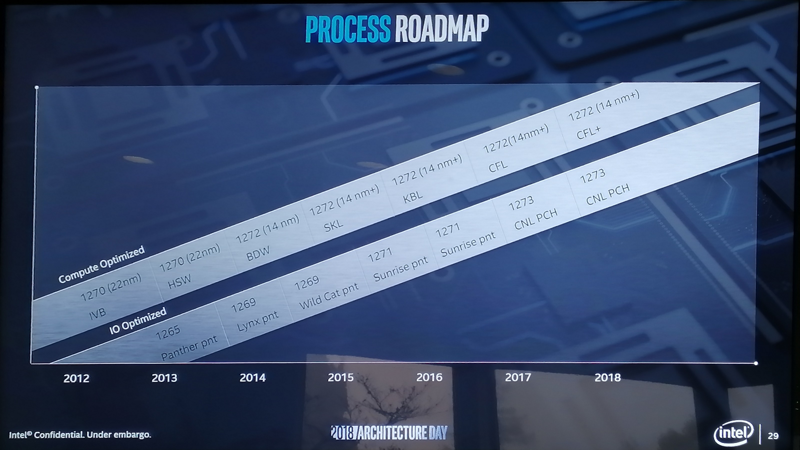
The 126x and 127x are the internal numbering systems for Intel’s process node technologies, although they don’t differentiate between BKM updates for the "+" node variants it turns out. But the point here is that Intel already knows that it needs certain process optimizations in place depending on the type of transistors, performance, and power needed. Going forward, Intel is going to be expanding its node base out so it can cover more power and performance points.
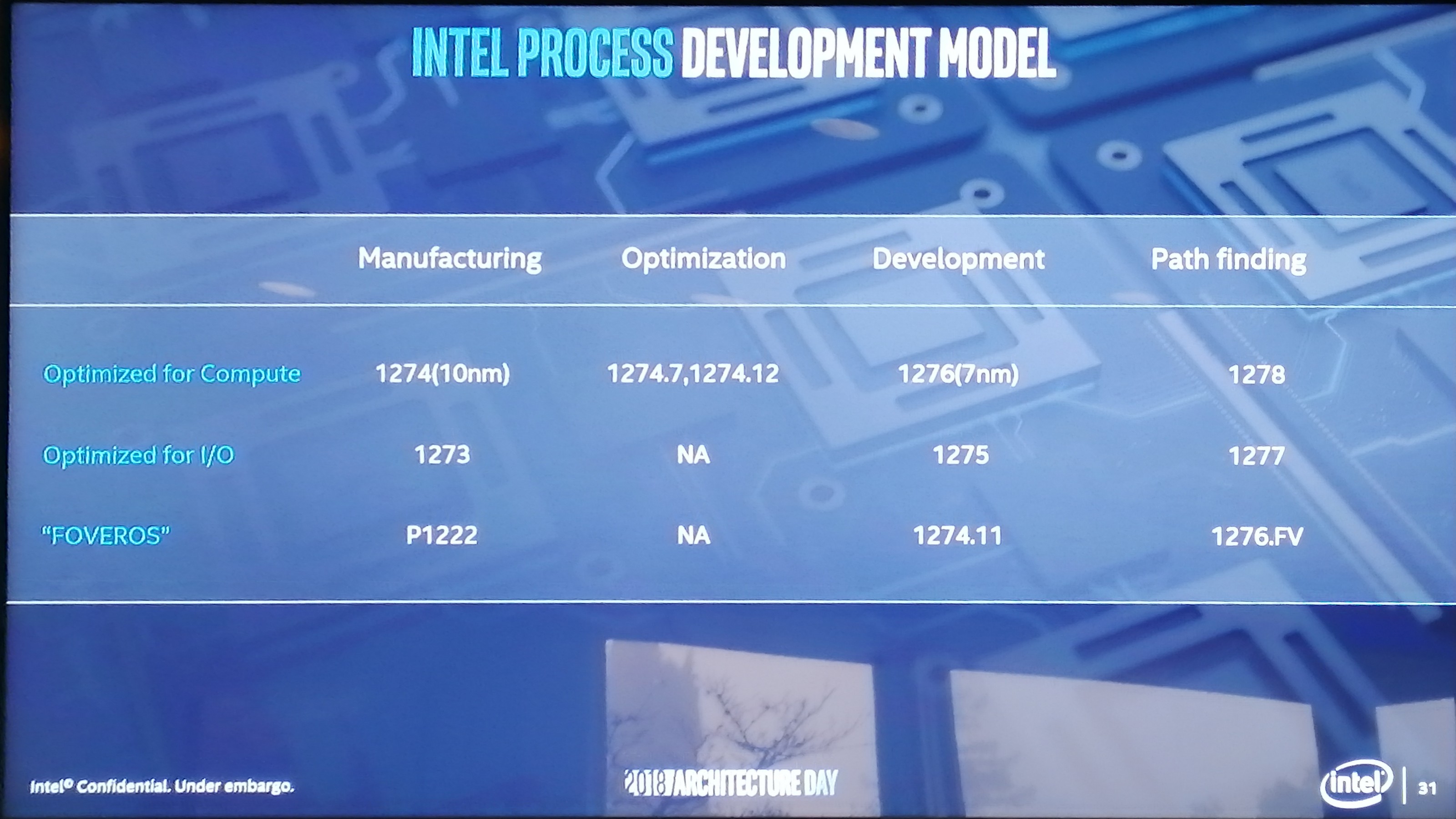
So for this example, Raja pulled out the current set of process technologies for 2019. For a manufacturing process, compute has the 1274 process on 10nm, IO has the 1273 process (14nm), while this new special Foveros technology is under P1222. Alongside the manufacturing, Intel will be working on optimizations focusing on the compute aspects of the manufacturing node. There will also be a set of developments for future node technologies, and the final column shows that Intel has path-finding research to look into future technologies and determine what capabilities will be possible on future designs. This sounds pretty much what a company like Intel should be doing, so no argument from me so far. The goal here is that each type of transistor use case can be different, and there isn’t a one-size fits all approach.

One way to assist with this is through chiplets and packaging. By picking the best transistor for the job in each case, whether it is CPU, GPU, IO, FPGA, RF, or anything else, with the correct packaging, it can be put together to get the best optimizations available.
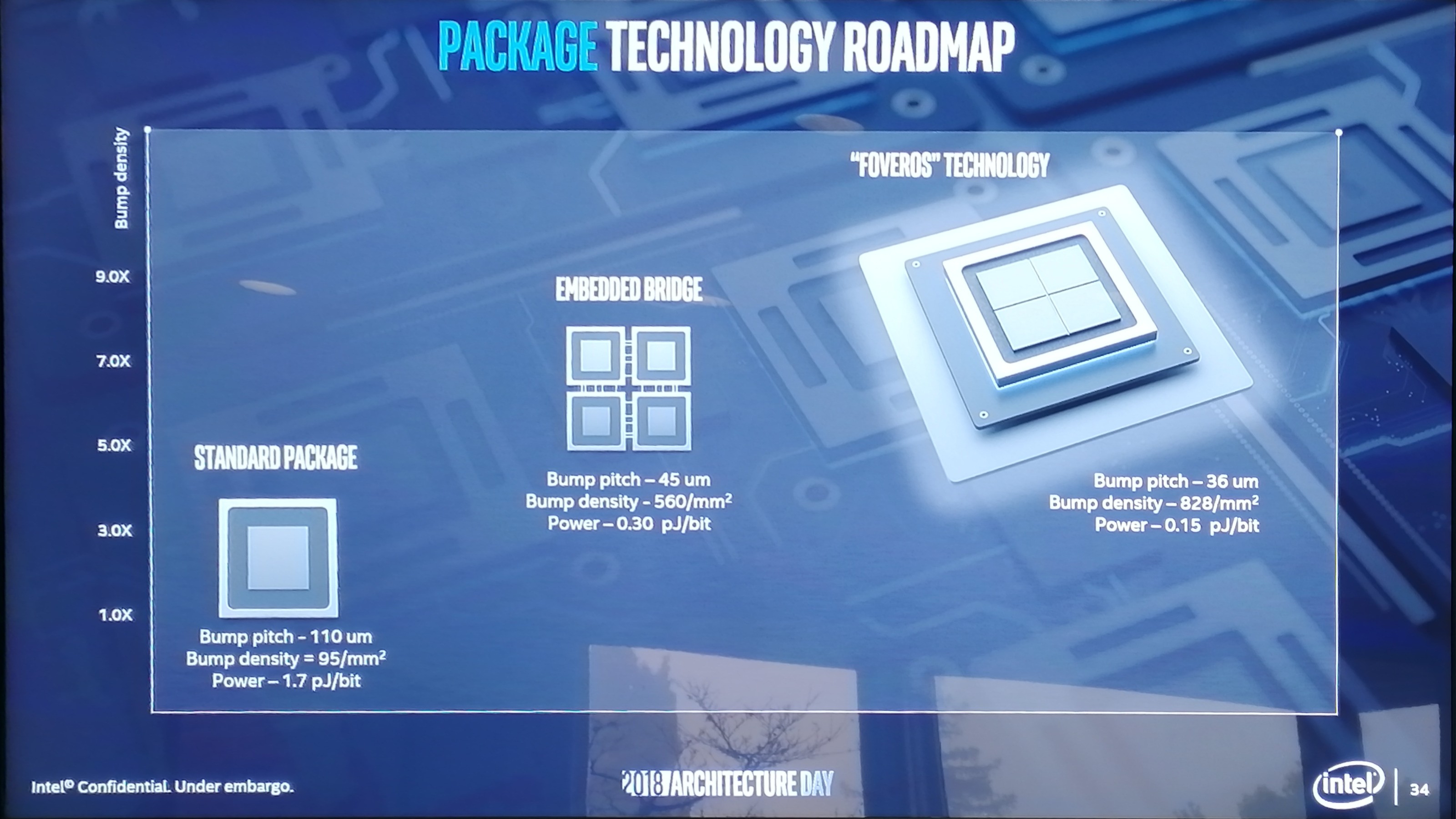
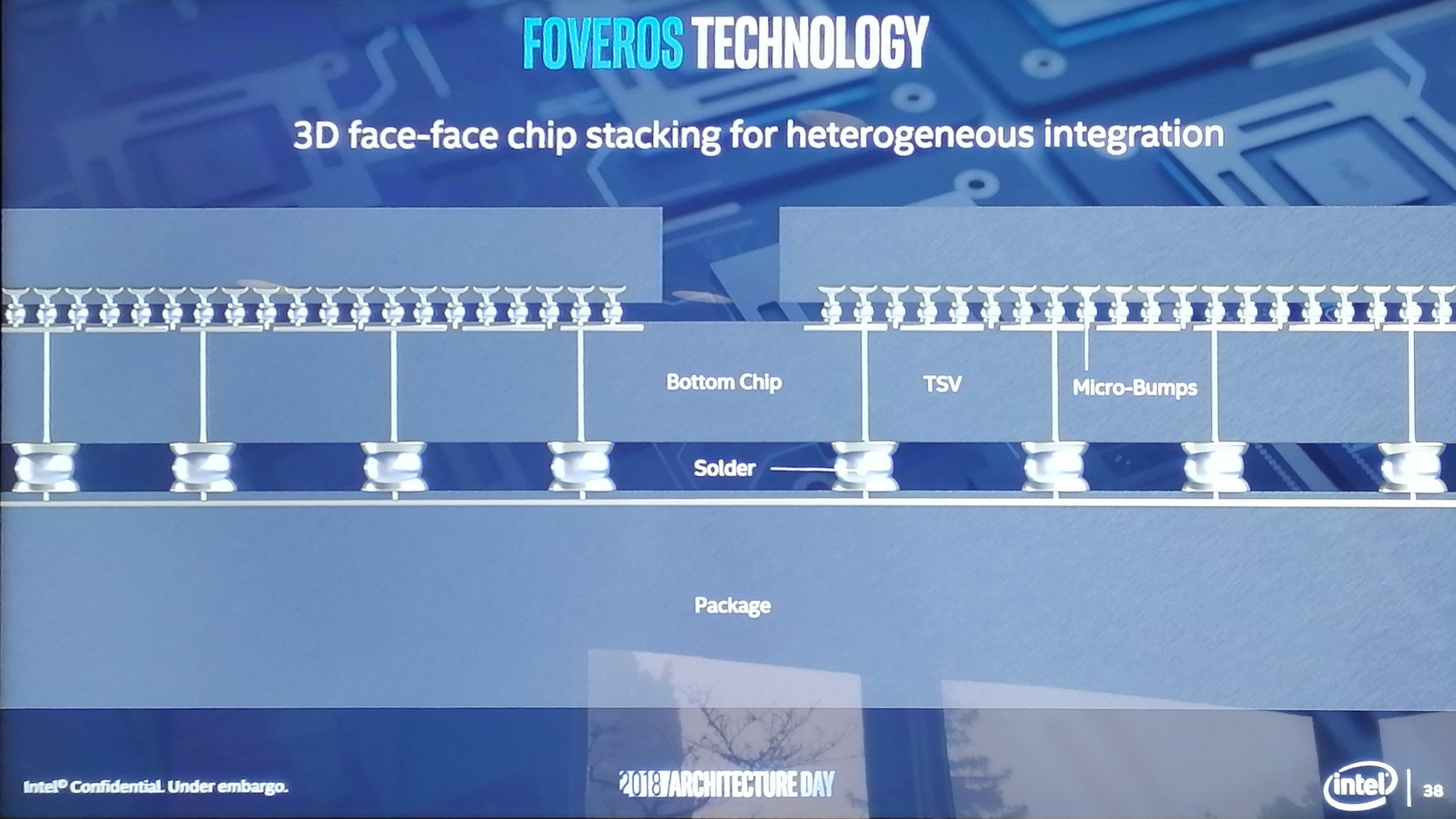
So here’s where Foveros fits in. Foveros is Intel’s new active interposer technology designed as a step above its own EMIB designs for small form-factor implementations, or those with extreme memory bandwidth requirements. For these designs the power per bit of data transferred is super low, however the packaging technology has to deal with the decreased bump pitch, the increased bump density, and also the chip stacking technology. Intel says that Foveros is ready for prime time, and they can produce it at scale.
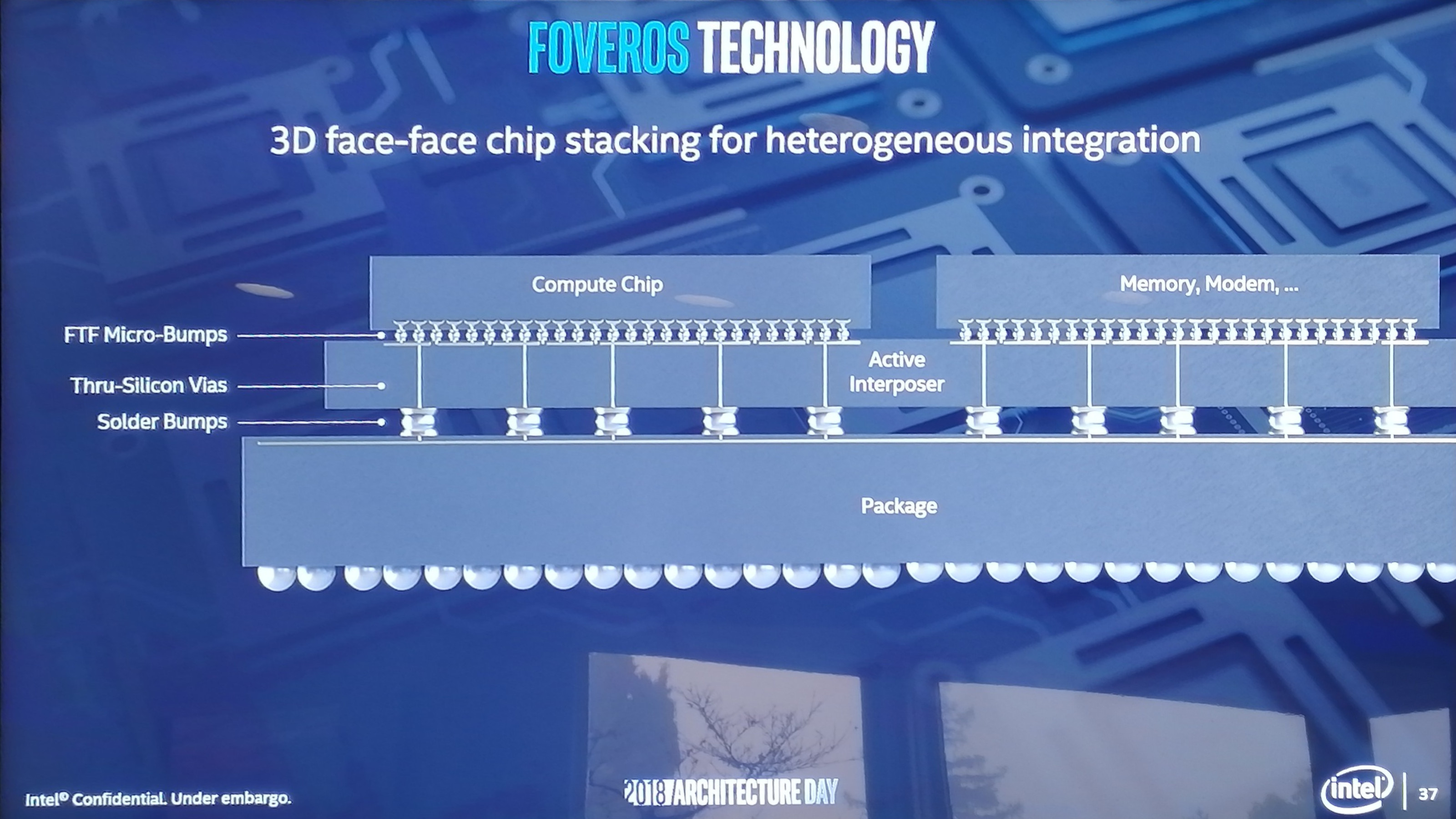
So this Foveros ‘3D’ packaging just sounds like a silicon interposer, such as what we’ve seen on AMD’s Fiji or NVIDIA’s high-end datacenter GPUs. However Intel is going above what those products are doing by actually making the interposer part of the design. The interposer contains the through-silicon vias and traces required to bring power and data to the chips on top, but the interposer also carries the PCH or IO of the platform. It is, in effect, a fully working PCH, but with vias to allow chips to be connected on top.
The first iteration of this technology is less complicated that the slide above, just using a set of CPU cores attached to the PCH below, but the idea is that a large interposer can have select functions on it and those can be removed from the chips above to save space. This also lets Intel use the different transistor types in different chips – the example we were given uses an interposer built on the 22FFL process node, with a 10nm set of CPUs on the top die. Above this, DRAM is provided in a POP package. Sounds cool, right?
In actual fact, Intel had a Foveros chip or two working in the demo area. These, Intel explained, were hybrid x86 designs that combined a single big Core with four smaller Atom cores on the same 10nm piece of silicon. I’m sure I’ve heard about big.Little before, but I was shocked that Intel is actually going to do it! We managed to take a photo of the block diagram, which Intel removed from its slide deck before sending it out to the press after the presentations. All details on the next page.


148 Comments
View All Comments
porcupineLTD - Thursday, December 13, 2018 - link
Can you articulate what you want to say with those links? or how they might contradict me/answer my question?ajc9988 - Thursday, December 13, 2018 - link
What I am saying with those links is that AMD has already evaluated the use of active interposers and is the company that is articulating a data protocol for active interposer routing so that it doesn't matter what each chiplet does on its own data routing, so that any chiplet could be attached to an active interposer and work. Further, in the 2017 white paper, it directly shows the reason that AMD hasn't yet adopted the active interposer is due to costs. Passive interposers can be used, but don't offer the benefit of active interposers. But, the cost of an active interposer is the same as doing a monolithic chip once the active interposer is produced on the 32nm or smaller active interposer. As such, adoption did not yet make sense until the costs are reduced.https://spectrum.ieee.org/tech-talk/semiconductors...
The earlier ones show AMD did research into the optimal topology for active interposers in 2014 and 2015. It shows the optimal core count for the benefit, latencies, etc.
Now, if you look at packaging solutions, say from GF, you find that 2.5D and 3D integration is only available on 32nm and 28nm processes, with 14nm coming soon. https://www.globalfoundries.com/sites/default/file...
I bring up GF doing the packaging as, due to the WSA, even if they cost more than competitors, being able to potentially count the wafers used for the active interposers against the WSA would reduce the fines payed under that contract for doing fabrication at TSMC, making it potentially, on net, cheaper.
Now, there is an article today from Anand saying Intel is releasing the B365 chipset on 22nm. ( https://www.anandtech.com/show/13714/intel-adds-b3... ) Intel was forced to move chipsets back to 22nm due to the 10nm process not being ready for mass deployment which caused a shortage of 14nm capacity. This means Intel could not shut down their 22nm fabs to cut that capacity. As such, a fab needs to stay as close to capacity as possible or else it bleeds money (hence why AMD eventually went fabless). So, Intel using 22nm fabs to do the 22nm active interposer is just Intel making lemonade on tech that few others adopted in the industry yet due to the basis of costs. If you go back to the cost study AMD did, the active interposer at 20nm is around the cost of doing a monolithic die, which is what Intel has done to date. So it isn't really costing them more to add in the active interposer at all, while saving expenditures by keeping the 22nm fabs full of jobs, while having awesome yields on the active interposers due to it being a very mature node with low defect rates, etc. If you examine the amount of area AMD estimated is needed for the logic routers, you can see only 1%-10% area on the active interposer is needed to achieve the goal, meaning the chances a critical defect hits the active interposer is very low.
But, as to it making AMD do it, that is the wrong thinking. AMD already plans to adopt it, just not until the costs of doing so are lower. They will check the IC Knowledge lists to see when costs make sense.
But, if you look at all that data I provided, AMD has all the solutions to the problems encountered with using an active interposer. All they are waiting for is it to be cost effective. Intel isn't leading anything here, other than doing it because they need to justify and subsidize having to keep certain 22nm fabs open because of their chipsets due to the delays in 10nm. Doesn't take a genius to figure it out, just takes someone paying attention to the tea leaves.
ajc9988 - Thursday, December 13, 2018 - link
Also, I forgot to mention that the 2.5D integration of HBM Phy onto a stitched interposer was accomplished last year. This suggests that HBM could be added to an active interposer when AMD eventually does adopt an active interposer. Meanwhile, with only 1-10% of the active interposer being used according to their papers, it leaves room for in the future having elements of the I/O chip being moved to the active interposer as an additional way that things easily could develop. The question is what benefit it would be to produce what on the 32nm or 28nm nodes over having their I/O disintegrated die on 14nm. But I would bet AMD has an idea of what would be better where and will consider it when eventually adopting, considered the detailed paper on routing topology of active interposers in that group of links.porcupineLTD - Thursday, December 13, 2018 - link
Thank you for the detailed response its very informative however its besides my comment, IF Intel ships its chiplet on interposer design in 2019 they will be first (regardless of the reasons or economics behind it), as for AMD not doing it now it's again besides my comment, I wandered if they will do this for ZEN 3 or 4 not ZEN2, ZEN 3 will launch in 2020 when (as far as I know) the WSA expires so what GF does or doesn't do is not that relevant (I would be curious to know about tsmc's or samsung's packaging/interposer offerings). The result (if they implement it in ZEN3/4) will come down to cost (as you point out), socket compatibility (can it be done on the current server socket?) and planning (ZEN3 design is almost done right now so even if the interposer cost is down AMD can't implement it if they didn't predict this one year ago).porcupineLTD - Thursday, December 13, 2018 - link
Also Anandtech, I am not versed in web design, but is it really that hard to have a comment section that doesn't utterly suck? Is it really that hard to introduce an edit function, or at least a delete one?(an upvote/donvote system would be asking for too much).ajc9988 - Thursday, December 13, 2018 - link
Forgive me, many think that Intel is showing through using it that they are significantly ahead in the field of active interposers and 2.5D and 3D chiplet integration, meaning that it would take years for other chip designers to catch up, which isn't the case. So I do apologize for that assumption in regards to you.What those do show is AMD does have plans to do so in the future, it is just a matter of timing. On the socket part, there is a chance they are introducing a new socket in order to support PCIe 4.0 on the upcoming Zen 2 chips, which comes from analyzing their wording from the Next Horizon event on Nov. 6th. Meanwhile, we know that PCIe 5.0 will be finalized potentially in the first half of next year and AMD did mention DDR5 potentially being available for Epyc 3 chips based on Zen 3, but that mainstream chips will not support DDR5 in 2020 (leaves open that TR HEDT platforms may or may not get DDR5 support at that time). Intel has not provided information on when PCIe 4.0, 5.0, or DDR5 will be supported. As such, though, AMD may have backwards compatibility on the CPUs for socket compatibility, but may require a new socket for the new boards containing the new features, which I think is understandable to many in the server and workstation spheres. It is also the reason I may wait for 2020 to upgrade my 1950X rather than next year (if you are going to buy a new board, and there is a chance that board won't contain the new feature sets that release that year, waiting one more year is fine IF your workloads won't suffer for the wait).
But, I read somewhere Intel hinted at 1GB of RAM being integrated with the active interposer processors, acting as an L4 cache. Although not novel (those articles I gave for AMD whitepapers from 2014 and 2015 specifically dealt with on package integration of memory and latencies involved, suggesting we could see some type of 3d memory solution integrated when AMD does incorporate an active interposer), seeing the latencies involved with Crystalwell, which was the eDRAM on Broadwell, suggests that Intel will get a significant uplift in certain workloads, as well as keeping the chip primed and having to go off chip less often for memory calls, which is fantastic. Intel also kept the power delivery part under wraps, which is something that does excite me, but we were given no information about it (possibly bringing FIVR back, which was rumored for Ice and Tiger lake anyways).
Also, on compatibility, part of the reason I gave the article discussing data protocols for active interposers is that the routing is chiplet agnostic, meaning you can integrate parts that have their own internal routing and not effect it. Then just comes down to appropriate socket wiring, which I mentioned they may need new sockets for these features, while just maintaining drop in compatibility for consumer side.
Here is some information on other packaging types out there in the market. I am including them, but as this is just being researched, I am not attesting veracity or relevance, fully. I will have glanced through them, but you understand.
http://s3.amazonaws.com/sdieee/1817-SanDiegoCPMTDL...
"DIGITIMES reports that the new TSMC plant in Chunan will be dedicated to offering the foundry’s in-house developed advanced packaging technologies: CoWoS (chip-on-wafer-on-substrate) and integrated fan-out (InFO) wafer-level packaging, and its newly-unveiled system-on-integrated-chips (SoIC) and wafer-on-wafer (WoW) packaging services."
https://criticalmaterials.org/tsmc-to-set-up-new-f...
https://fudzilla.com/news/pc-hardware/47265-tsmc-t...
https://electroiq.com/2018/10/synopsys-design-plat...
Older article for foundational work from 2014:
https://semiengineering.com/time-to-revisit-2-5d-a...
2016 follow up: https://semiengineering.com/2-5d-becomes-real/
Packaging Market from February 2018:
http://worldherald24.com/2018/02/19/global-3d-ic-a...
Paper and slide show discussing the implementation and challenges of 3D packaging from 2016:
https://smtnet.com/library/files/upload/25d-3d-sem...
Sorry for the data dump at the end. I do apologize about that.
tommybobberson - Saturday, December 15, 2018 - link
just clarifying, do you mean to use such methods, amd would need to rive up production costs which reduces their profit/value. but since intel already has a high production cost, such methods would not affect them?ajc9988 - Wednesday, December 19, 2018 - link
tommybobberson - in a manner of speaking, yes. How much it costs to produce effects margins and pricing. One reason AMD could price the high core chips in such a manner, aside from effective yields for products, is the decreased costs to produce high core count products. If AMD added the active interposer now, it would rise production costs to be the same as a monolithic die, which would then require either an increase in market price of the products or a decrease in margins for their products.Intel, on the other hand, never captured the extra margin of going to chiplets before introducing the stacked chips. That means that the active interposer cost to them is less as the price to do so matches the cost of a monolithic die. As such, Intel can maintain their current pricing while introducing the stacked die on active interposer. Further, due to filling up 22nm fab time (because of 10nm causing a shortage of 14nm fab time which required Intel to move certain lines back to 22nm, likely forcing some plants planned to be closed or retrofitted to remain on 22nm), Intel will be able to help on the cost of 10nm delay, thereby mitigating some of the effects found in not having 10nm up and running by now.
Supercell99 - Friday, December 14, 2018 - link
With all the hackers, PC gaming is dying.sgeocla - Wednesday, December 12, 2018 - link
Fist they mock your chiplets by saying you glue your dies together, then they fail to compete with you and then years after they copy your chiplets and call it revolutionary.This is why Intel can no longer have public presentations of their own failures and have to have privately controlled presentations.