Intel's Architecture Day 2018: The Future of Core, Intel GPUs, 10nm, and Hybrid x86
by Dr. Ian Cutress on December 12, 2018 9:00 AM EST- Posted in
- CPUs
- Memory
- Intel
- GPUs
- DRAM
- Architecture
- Microarchitecture
- Xe
The Next Generation Gen11 Graphics: Playable Games and Adaptive Sync!
Some of the first words out of the mouth of Raja Koduri about graphics is that Intel has a duty to its one billion customers with integrated graphics to give them something that is useful, and that it is time for Intel to provide graphics which people can actually play games on. Given his expertise on the matter, it shouldn’t sound too far-fetched: more people play games than ever before, and these users want to play no matter what their hardware. To that end, Raja stated that Gen11 graphics is the first step in a new graphics policy to provide the performance and features to let gamers play the most popular games, no matter what implementation.
Gen11: Intel’s first GT2 TFLOPS Graphics
In 2015, Intel launched the Skylake processor with Gen9 integrated graphics. Rather than moving straight to Gen10 the next time around, we were given Gen 9.5 in both Kaby Lake and Coffee Lake, which supposedly draw features from what would have been Gen 10. Actually, the graphics for Intel’s failed 10nm Cannon Lake chip were meant to be called Gen10, however Intel never released a Cannon Lake processor with working integrated graphics, and because Gen11 goes above and beyond what Gen10 would have been, we’ve gone straight to Gen11. Make sense? Well Intel didn’t even bother to acknowledge Gen10 in its history graph:

We will see Gen11 graphics being paired with Sunny Cove cores on 10nm sometime in 2019 according to the roadmaps. However rather than give a detailed architecture layout for the new product, we instead were given a rather high level diagram.
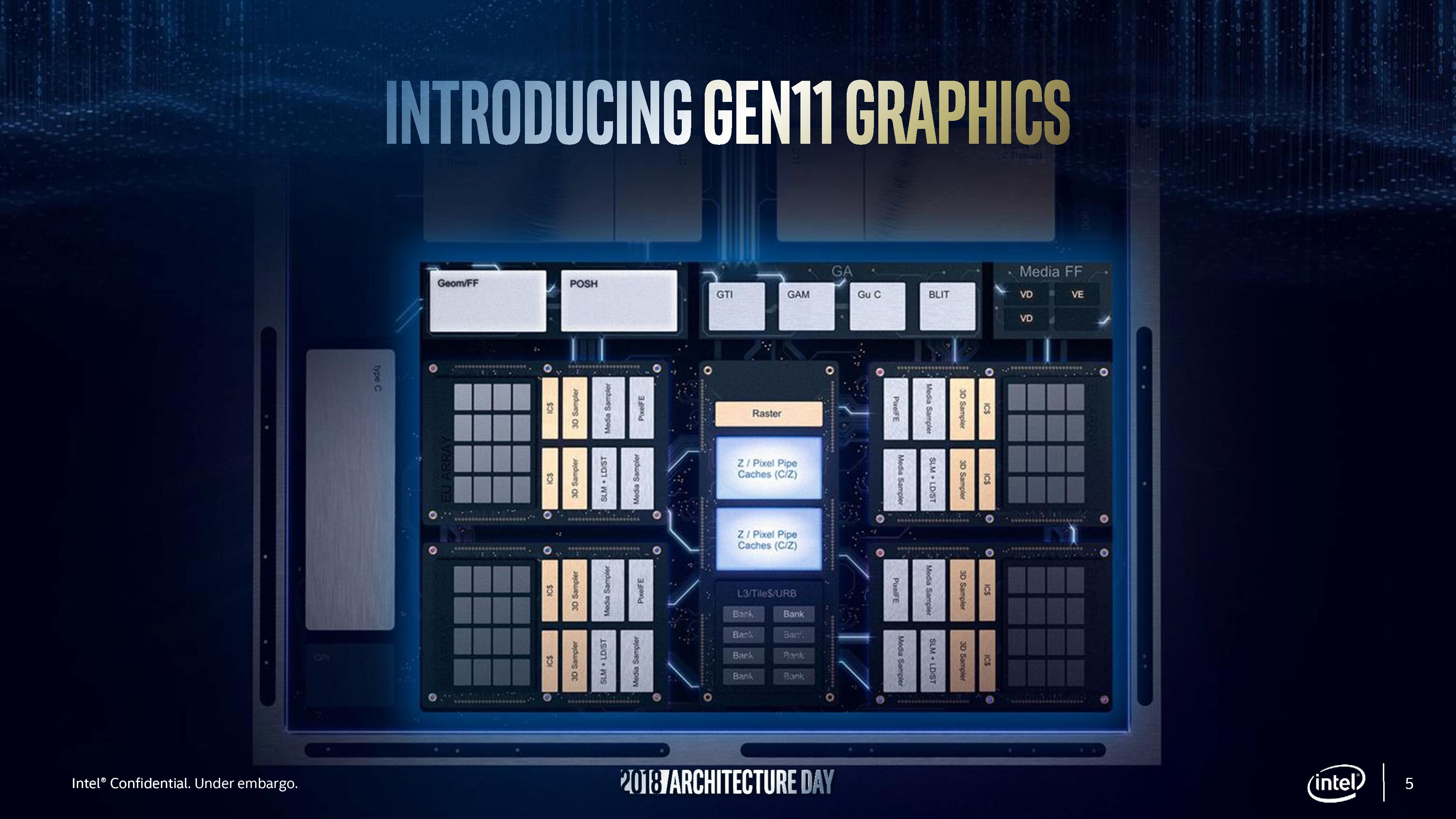
From here we can deduce a few things. We were told that this configuration is the GT2 config, which will have 64 execution units, up from 24 in Gen9.5. These 64 EUs are split into four slices, with each slice being made of two sub-slices of 8 EUs a piece. Each sub-slice will have an instruction cache and a 3D sampler, while the bigger slice gets two media samplers, a PixelFE, and additional load/store hardware. Intel lists Gen11 targeting efficiency, performance, advanced 3D and media capabilities, and a better gaming experience.
Intel didn’t go into too much detail regarding how the EUs are at higher performance, however the company did say that the FPU interfaces inside the EU are redesigned and it still has support for fast (2x) FP16 performance as seen in Gen9.5. Each EU will support seven threads as before, which means that the entire GT2 design will essentially have 512 concurrent pipelines. In order to help feed these pipes, Intel states that it has redesigned the memory interface, as well as increasing the L3 cache of the GPU to 3 MB, a 4x increase over Gen9.5, and it is now a separate block in the unslice section of the GPU.
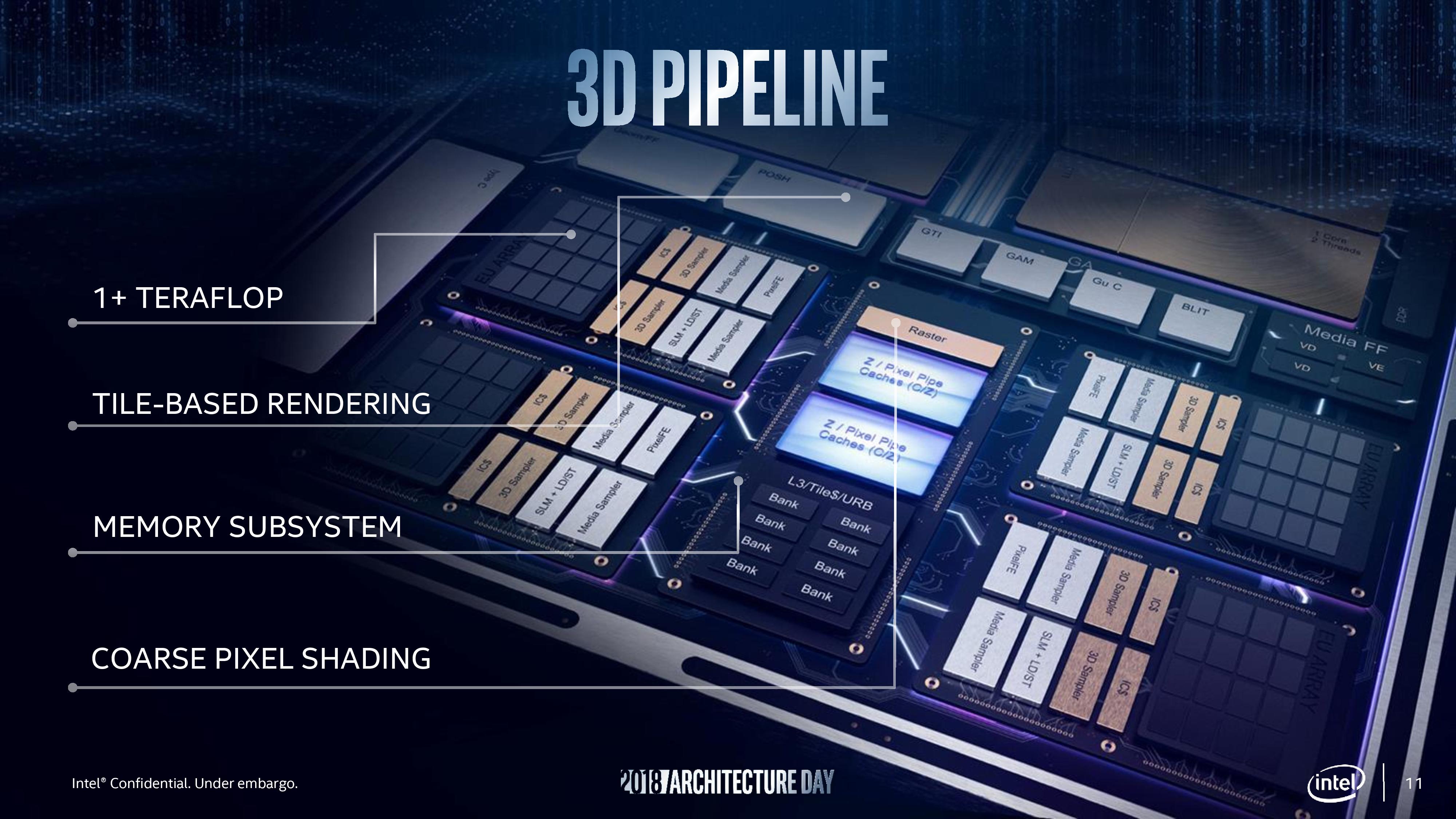
Other features include tile-based rendering, which Intel stated the graphics hardware will be able to enable/disable on a render pass basis. This will make Intel the final member of the PC GPU vendor community to implement this, following NVIDIA in 2014 and AMD in 2017. While not a panacea to all performance woes, a good tile rendering setup plays well to the bandwidth limitations of an integrated GPU. Meanwhile Intel's lossless memory compression has also improved, with Intel listing a best case performance boost of 10% or a geometric mean boost of 4%. The GTI interface now supports 64 bytes per clock read and write to increase throughput, which works with the better memory interface.
Coarse Pixel Shading, Intel's implementation of multi-rate shading and similar in scope to NVIDIA’s own Variable Pixel Shading, is also supported. This allows the GPU to reduce the amount of total shading work required by shading some pixels on a less than 1:1 basis. Intel showed two demos for CPS, where pixel shading was reduced either as a function of object distance from camera (so you do less work when things are further away), or reduced as a function of how close the object is to the center of the screen, designed to help features like foveated rendering for VR. With a 2x2 pixel stencil applied – meaning only one pixel shading operation was done per block of 4 pixels – Intel stated a ~30% increase in frame rates in supported games. Unfortunately this needs to be applied on a game-by-game basis in order to prevent significant image quality losses, so the performance gains won't be immediate or universal.
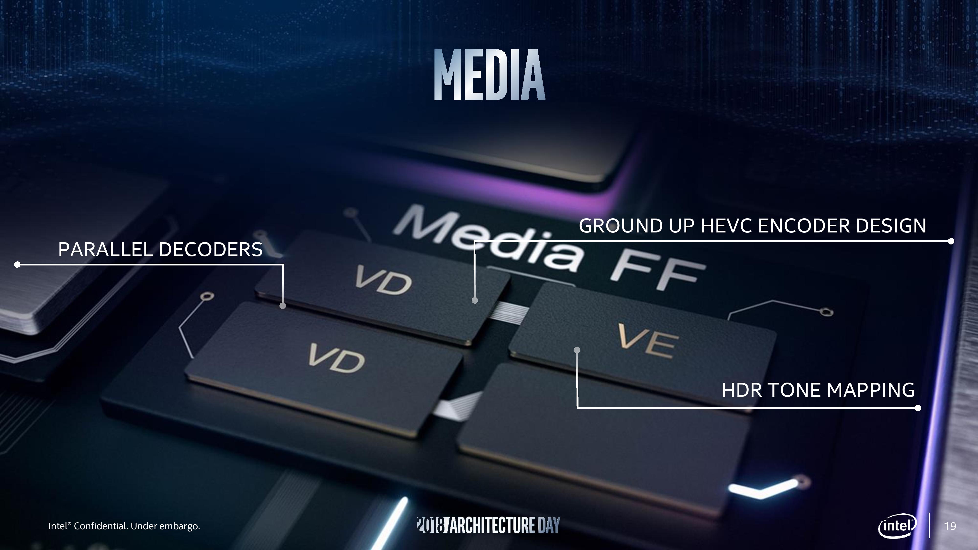
For the media block, Intel says that the Gen11 design includes a ground up HEVC encoder design, with high quality encode and decode support. Intel cited the fact that its media fixed function units are already used in the datacenter for video processing, and home users can take advantage of the same hardware. Intel also stated that by using parallel decoders it can either support concurrent video streams or they can be combined to support a single large stream, and this scalable design will allow future hardware to push the peak resolutions up to 8K and beyond.

The highlight of the display engine is support for Adaptive Sync technologies. We were told that it was announced back at the launch of Skylake, but now it is finally ready to go into Intel’s integrated graphics. This goes in hand with HDR support due to its high-precision data path.
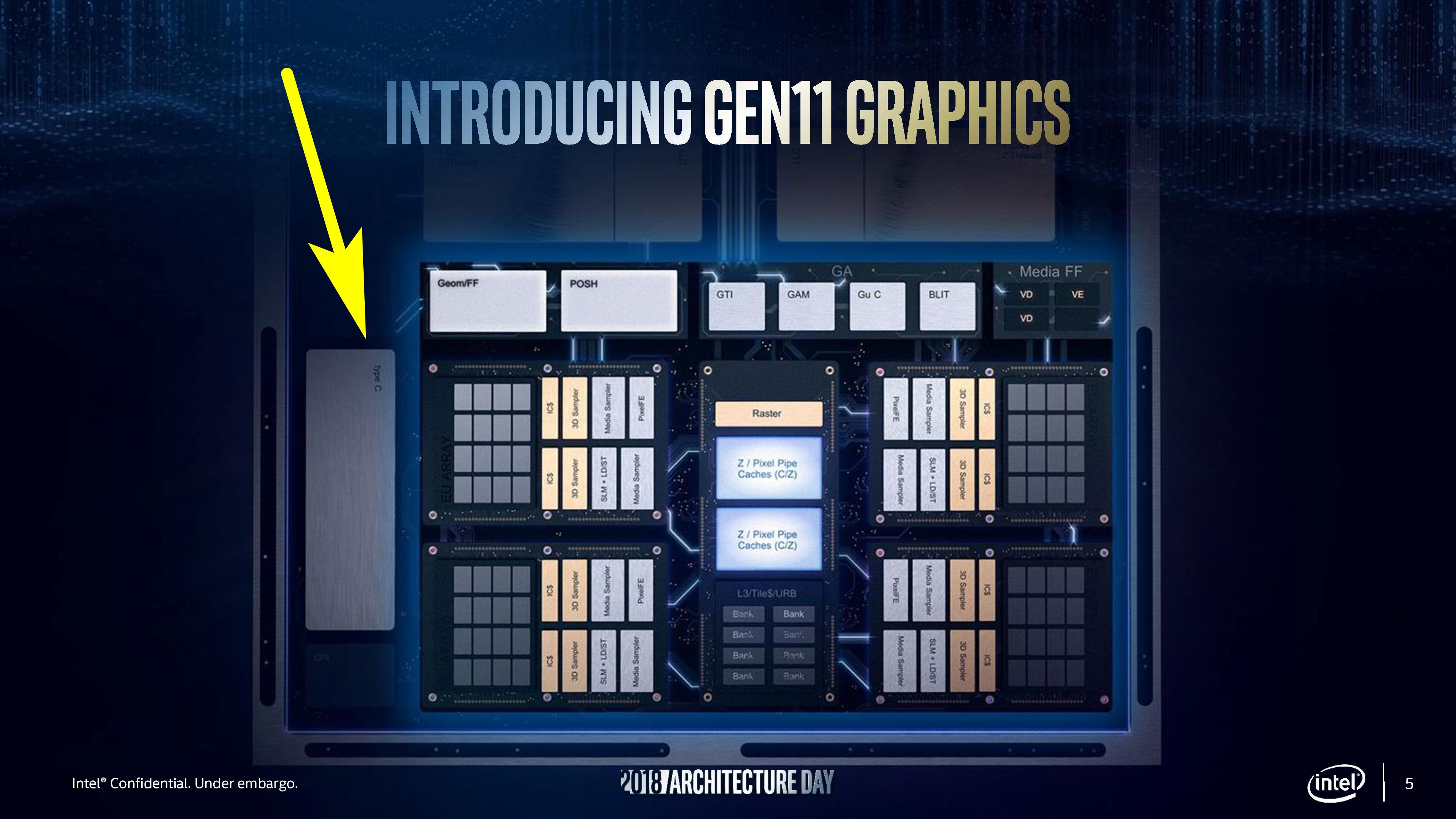
One thing in this presentation that Intel didn’t mention directly is that Gen11 graphics would appear to have Type-C video output support, potentially indicating that Intel has integrated the necessary mux into the chipset itself, removing another IC from the motherboard design.


148 Comments
View All Comments
johannesburgel - Wednesday, December 12, 2018 - link
"We have a new method inside the company to decouple IP from the process technology. You must remember that customers buy the product, not a transistor family. It’s the same transformation AMD had to go through to change the design methodology when they were struggling."...doesn't that basically mean they're going fabless, or are at least going to develop a design for multiple processes so they can also use other fabs as well? Not that I'm disagreeing with that! If I was Intel I would have started doing so years ago, when everybody else was starting to do it.
anonomouse - Wednesday, December 12, 2018 - link
I think this just means fewer hand placed/routed custom logic blocks, and more synthesis/APR. If you look at most other dies these days, you see a sea of gates. When you look at intel dies, in the cpu cores you see very tight, regular logic blocks. Every mention of "abstraction" in the Q&A screamed synthesis/APR. This may make it possible for them to port to other foundries if they wanted to, but I doubt they would.An interesting question is whether this has any implications to power/timing/area optimization vs. the current approach, as a lot of their ability to push very high clocks might come from how much more custom logic design goes into their implementation.
kapg - Wednesday, December 12, 2018 - link
I guess in the image Intel 'CPU Core Roadmap' for Atom the name 'Next' Month is a typo from IntelAlexvrb - Wednesday, December 12, 2018 - link
"quad-channel memory controller (4x16-bit)"Well, we know the GPU won't be competitive with upcoming ARM designs, then. Otherwise, very neat mobile class chip design.
Arbie - Wednesday, December 12, 2018 - link
"Golden Cove ... is firmly in that 2021 segment ... we’re likely to see it on 10nm and or 7nm."Likely? If it isn't one of those two it will be big news indeed.
HStewart - Thursday, December 13, 2018 - link
10nm is already stated for Sunny Cove in 2019, so it likely 7nm - but keep in mind the process (nm) is decouple for process - so it could be 10nm or 7nmajc9988 - Wednesday, December 12, 2018 - link
Ian, the active interposer isn't new, and I am wanting o know more exactly what has been moved to the active interposer. AMD's whitepapers on the topic, using routers, etc., on an active interposer, was published in 2014 and a follow up on 2015. In late 2017, AMD published a white paper dealing with the costs of doing so, where producing an active interposer on smaller than 40nm resulted in costs being the same as producing a monolithic die. AdoredTV did two videos on this topic months ago, as a matter of fact. So, unless they are sticking some of the features that AMD put on the I/O die onto the active interposer, this is doing what AMD plans to do but chose not to on the basis of cost. Check out these papers and videos:http://www.eecg.toronto.edu/~enright/micro14-inter... http://www.eecg.toronto.edu/~enright/Kannan_MICRO4... https://youtu.be/G3kGSbWFig4 https://seal.ece.ucsb.edu/sites/seal.ece.ucsb.edu/... https://www.youtube.com/watch?v=d3RVwLa3EmM&t=...
Intel seems to now be using ideas from everywhere else in the industry, while also using 22nm fabs that would have been slated for decommission if not for the 10nm fiasco that is their process, which they had to push certain chipsets to due to the 14nm shortage, meaning they need to keep the fab time full to justify them keeping the lights on and a 22nm active interposer fits the bill. The article practically writes itself.
iwod - Thursday, December 13, 2018 - link
No news on opening up TB3? Which they promised to do in 2018.The Hybrid, I wish it had two HP Core. but 7W is actually the same TDP for MacBook Air Retina.
The_Assimilator - Thursday, December 13, 2018 - link
Thunderbolt is dead in mainstream PCs at this point, because there's no use-case in which it outperforms USB by enough to justify its cost (both of implementation and in the peripherals that people actually want to use). It's become another almost-Mac-exclusive like Firewire, and will share the same fate.gamerk2 - Thursday, December 13, 2018 - link
Yep, this pretty much the same thing that happened to Firewire. Thunderbolt never had a reason to exist; USB3 handles pretty much every TB3 use-case.