Intel's Architecture Day 2018: The Future of Core, Intel GPUs, 10nm, and Hybrid x86
by Dr. Ian Cutress on December 12, 2018 9:00 AM EST- Posted in
- CPUs
- Memory
- Intel
- GPUs
- DRAM
- Architecture
- Microarchitecture
- Xe
The Next Generation Gen11 Graphics: Playable Games and Adaptive Sync!
Some of the first words out of the mouth of Raja Koduri about graphics is that Intel has a duty to its one billion customers with integrated graphics to give them something that is useful, and that it is time for Intel to provide graphics which people can actually play games on. Given his expertise on the matter, it shouldn’t sound too far-fetched: more people play games than ever before, and these users want to play no matter what their hardware. To that end, Raja stated that Gen11 graphics is the first step in a new graphics policy to provide the performance and features to let gamers play the most popular games, no matter what implementation.
Gen11: Intel’s first GT2 TFLOPS Graphics
In 2015, Intel launched the Skylake processor with Gen9 integrated graphics. Rather than moving straight to Gen10 the next time around, we were given Gen 9.5 in both Kaby Lake and Coffee Lake, which supposedly draw features from what would have been Gen 10. Actually, the graphics for Intel’s failed 10nm Cannon Lake chip were meant to be called Gen10, however Intel never released a Cannon Lake processor with working integrated graphics, and because Gen11 goes above and beyond what Gen10 would have been, we’ve gone straight to Gen11. Make sense? Well Intel didn’t even bother to acknowledge Gen10 in its history graph:

We will see Gen11 graphics being paired with Sunny Cove cores on 10nm sometime in 2019 according to the roadmaps. However rather than give a detailed architecture layout for the new product, we instead were given a rather high level diagram.
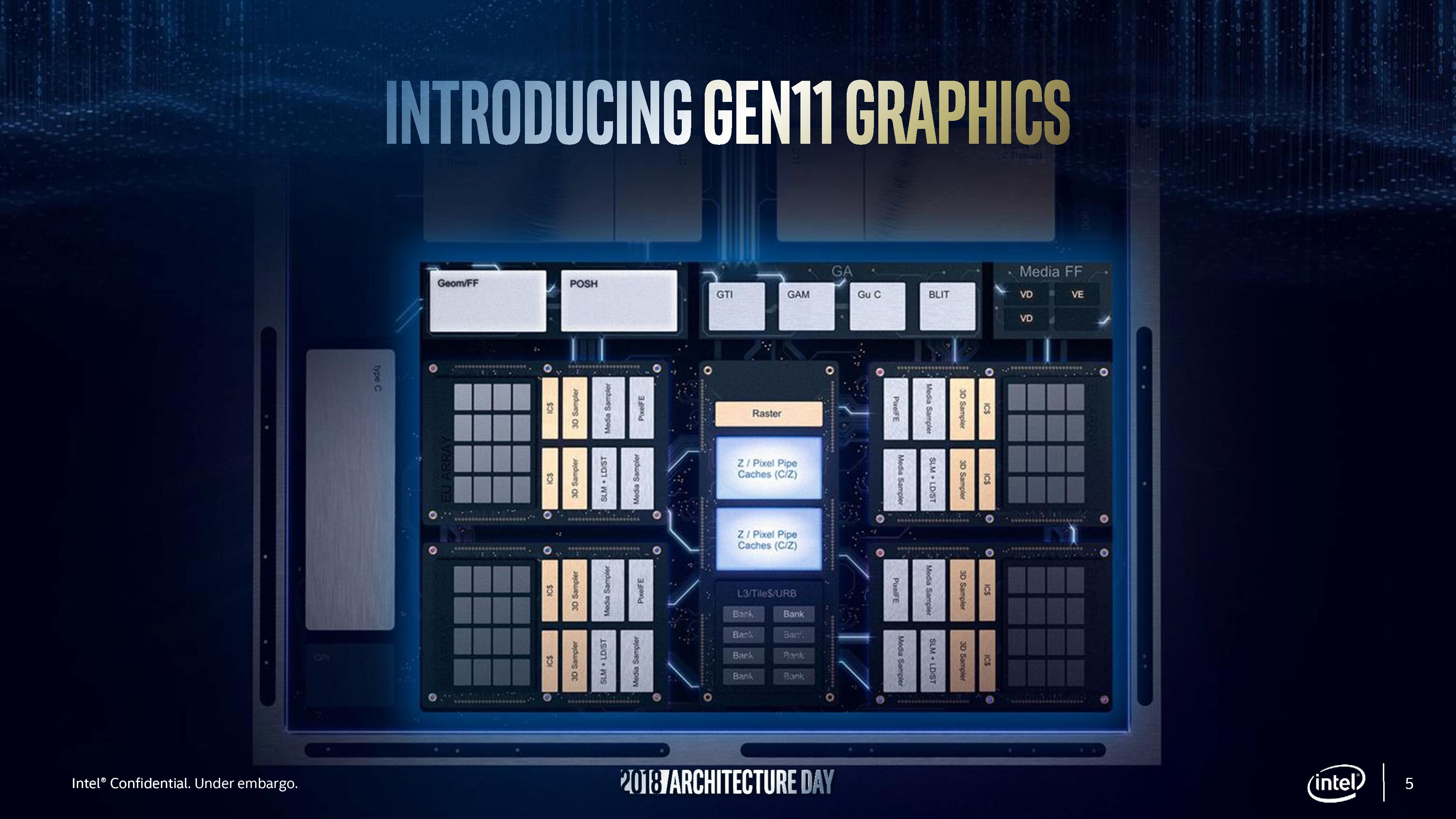
From here we can deduce a few things. We were told that this configuration is the GT2 config, which will have 64 execution units, up from 24 in Gen9.5. These 64 EUs are split into four slices, with each slice being made of two sub-slices of 8 EUs a piece. Each sub-slice will have an instruction cache and a 3D sampler, while the bigger slice gets two media samplers, a PixelFE, and additional load/store hardware. Intel lists Gen11 targeting efficiency, performance, advanced 3D and media capabilities, and a better gaming experience.
Intel didn’t go into too much detail regarding how the EUs are at higher performance, however the company did say that the FPU interfaces inside the EU are redesigned and it still has support for fast (2x) FP16 performance as seen in Gen9.5. Each EU will support seven threads as before, which means that the entire GT2 design will essentially have 512 concurrent pipelines. In order to help feed these pipes, Intel states that it has redesigned the memory interface, as well as increasing the L3 cache of the GPU to 3 MB, a 4x increase over Gen9.5, and it is now a separate block in the unslice section of the GPU.
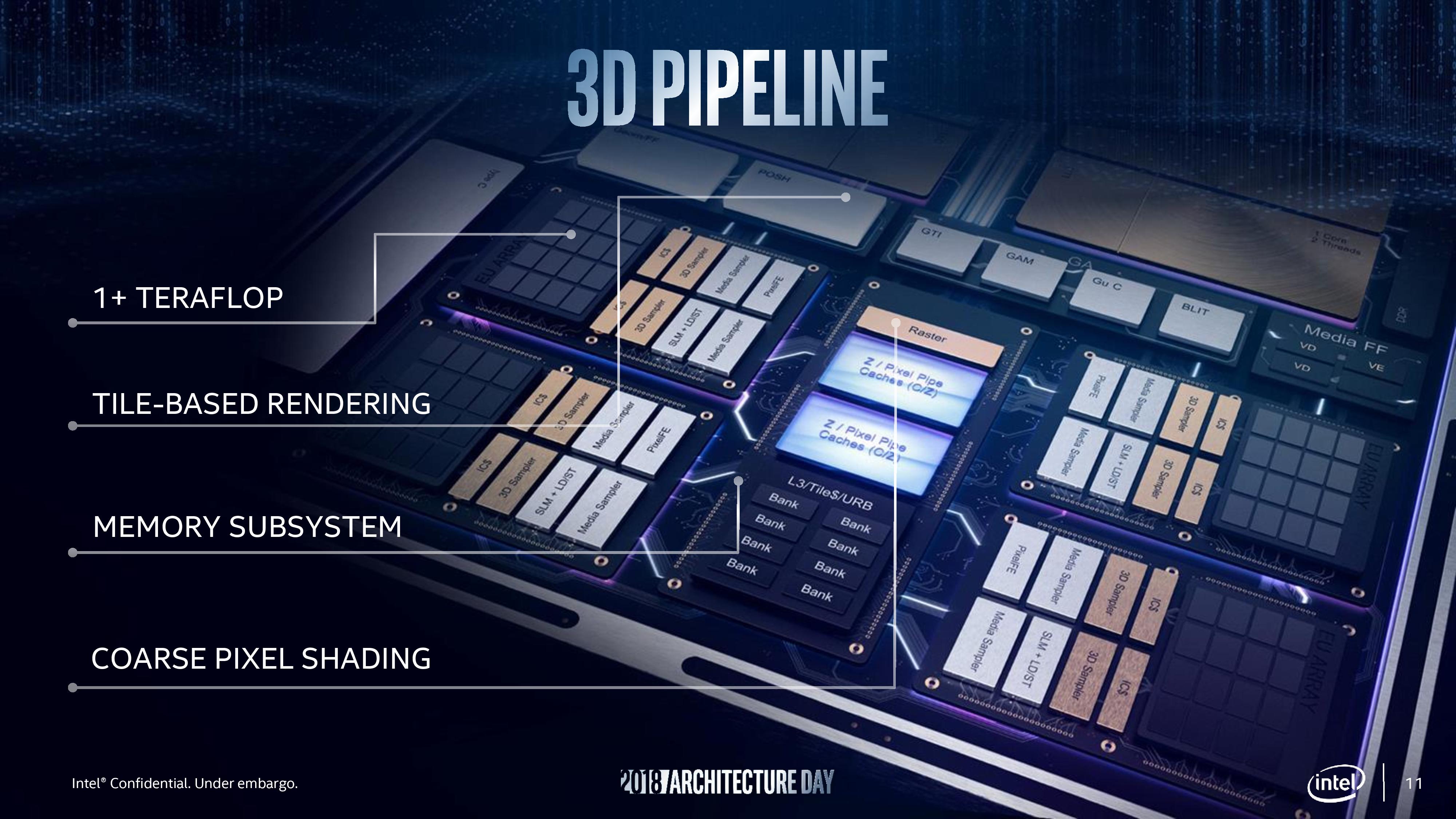
Other features include tile-based rendering, which Intel stated the graphics hardware will be able to enable/disable on a render pass basis. This will make Intel the final member of the PC GPU vendor community to implement this, following NVIDIA in 2014 and AMD in 2017. While not a panacea to all performance woes, a good tile rendering setup plays well to the bandwidth limitations of an integrated GPU. Meanwhile Intel's lossless memory compression has also improved, with Intel listing a best case performance boost of 10% or a geometric mean boost of 4%. The GTI interface now supports 64 bytes per clock read and write to increase throughput, which works with the better memory interface.
Coarse Pixel Shading, Intel's implementation of multi-rate shading and similar in scope to NVIDIA’s own Variable Pixel Shading, is also supported. This allows the GPU to reduce the amount of total shading work required by shading some pixels on a less than 1:1 basis. Intel showed two demos for CPS, where pixel shading was reduced either as a function of object distance from camera (so you do less work when things are further away), or reduced as a function of how close the object is to the center of the screen, designed to help features like foveated rendering for VR. With a 2x2 pixel stencil applied – meaning only one pixel shading operation was done per block of 4 pixels – Intel stated a ~30% increase in frame rates in supported games. Unfortunately this needs to be applied on a game-by-game basis in order to prevent significant image quality losses, so the performance gains won't be immediate or universal.
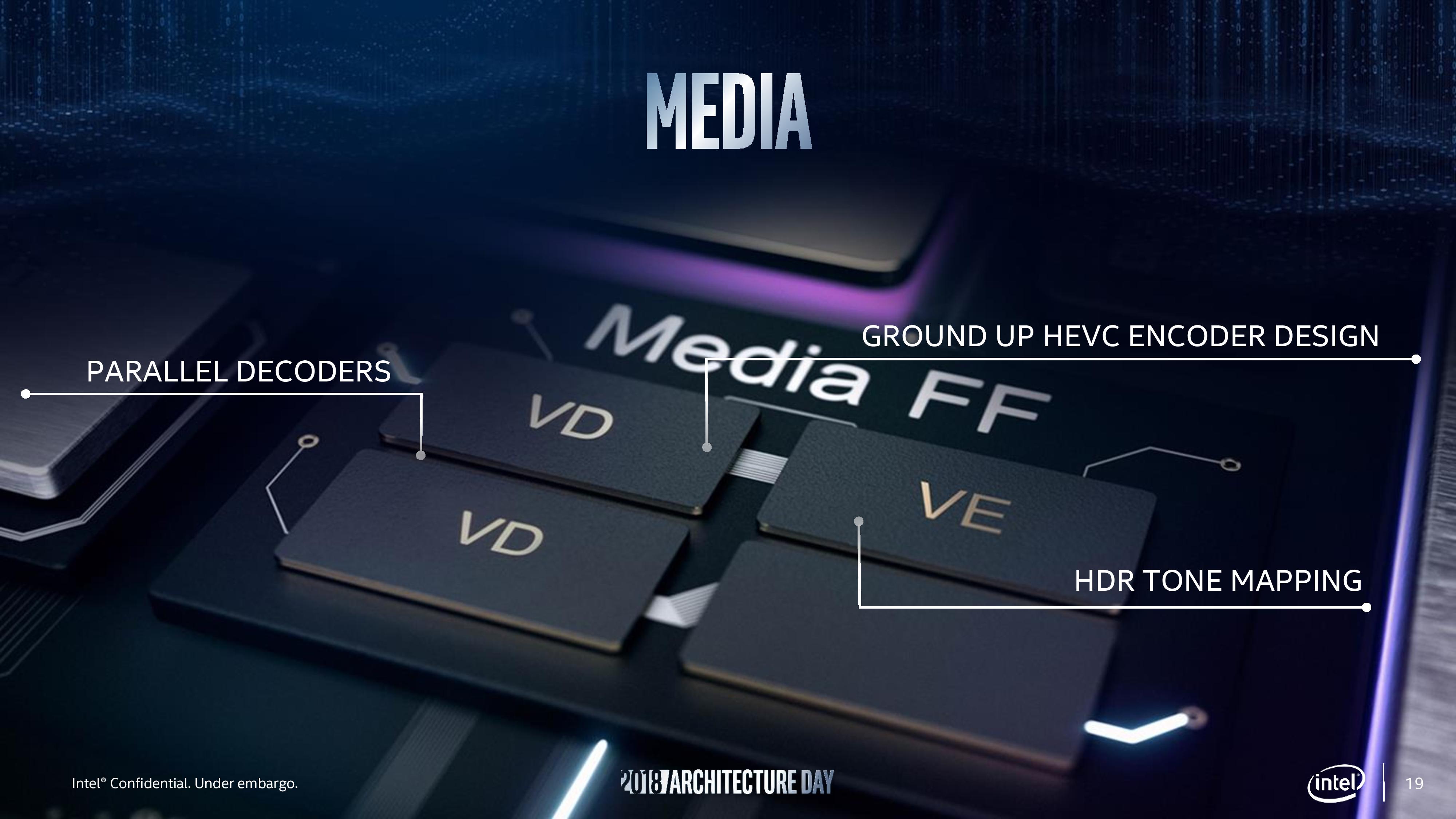
For the media block, Intel says that the Gen11 design includes a ground up HEVC encoder design, with high quality encode and decode support. Intel cited the fact that its media fixed function units are already used in the datacenter for video processing, and home users can take advantage of the same hardware. Intel also stated that by using parallel decoders it can either support concurrent video streams or they can be combined to support a single large stream, and this scalable design will allow future hardware to push the peak resolutions up to 8K and beyond.

The highlight of the display engine is support for Adaptive Sync technologies. We were told that it was announced back at the launch of Skylake, but now it is finally ready to go into Intel’s integrated graphics. This goes in hand with HDR support due to its high-precision data path.
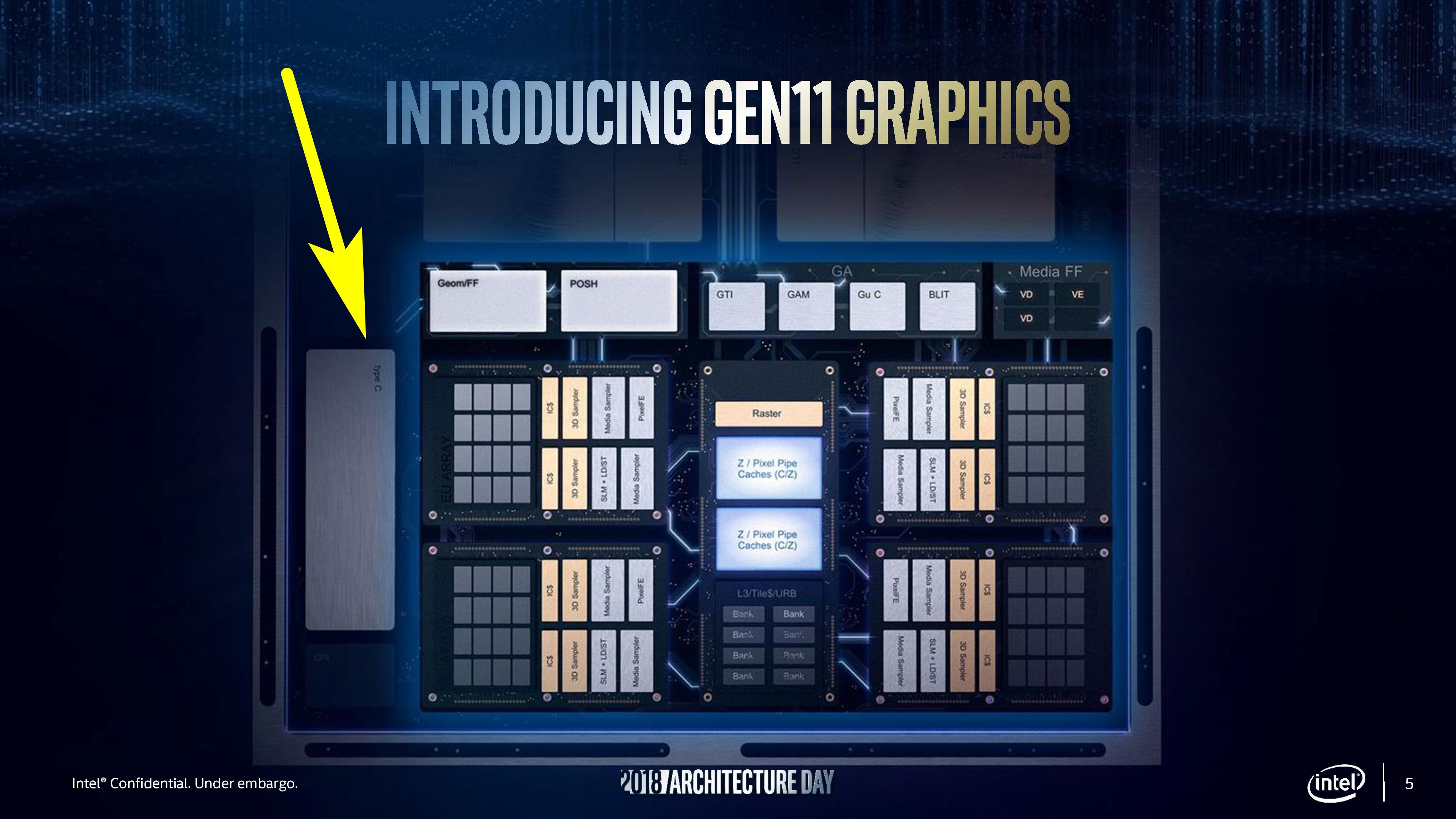
One thing in this presentation that Intel didn’t mention directly is that Gen11 graphics would appear to have Type-C video output support, potentially indicating that Intel has integrated the necessary mux into the chipset itself, removing another IC from the motherboard design.


148 Comments
View All Comments
ajc9988 - Thursday, December 13, 2018 - link
https://www.anandtech.com/show/13445/tsmc-first-7n...Risk production is in Q2 next year. And Mass is listed by Q2 2020 for 5nm.
https://www.extremetech.com/mobile/278800-tsmc-exp...
So, I was a bit off by the estimate for volume being 2020, but you were off on when risk production starts. Meanwhile, 7nm+ is already confirmed for AMD on Zen3, as the benefits of 5nm+ don't outweigh the costs associated moving to the process for AMD. This is why it is thought AMD will skip 5nm and try 3nm when available. But, TSMC has not said when 3nm will be available, while Samsung is saying 3nm in 2021:
https://semiengineering.com/big-trouble-at-3nm/
https://www.cdrinfo.com/d7/content/samsung-details...
http://www.semimedia.cc/?p=2524 (saying TSMC 3nm in 2022/23)
I cannot find the article speculating Apple will be the first customer on 5nm EUV and when ATM.
HStewart - Thursday, December 13, 2018 - link
"Nodes are marketing jargon"Exactly - it reminds me the frequence wars back in P4 days. But if you look closely at Intel's plan - I am no chip designer - even though I did take Micro-code Enginnering classes in College, but Foveros is revolutionary design - I thought EMiB was amazing, but to do that in 3rd diminsion is awesome - maybe one they could even stack cores that way - instead huge chip monsters.
But a nm rating by vendor 1 does not nm rating by vendor 2 - what underneath makes the different - Intel is extremely smart to decouple nm process from actual archexture. If you notice by Intel archiexture Intel has more improvements in core archiexture over next 3 years - this is because they are not limited by process (nm)
ajc9988 - Friday, December 14, 2018 - link
EMIB was not revolutionary and neither is foveros. They are incremental steps and existing competing solutions are available and have been for some time. Not only that, it will only be used on select products with eventual spread to the stack.Go to the second page of comments and see my links there. I think you will find those quite interesting. Not only that, this has been done with HBM for years now. If you look at AMD's research, almost half a decade ago, they were studying optimal topologies for active interposers. They found only 1-10% of the area was needed for the logic routing of an active interposer. Moving a couple I/O items onto the active interposer just is an extension. In fact, you can put those components on a spread out interposer between the above chiplets that sit on the interposer, but would need to plan on the heat dissipation or having so low a heat that it doesn't need sinked.
Considering lack of details of what is on the active interposer or timeline for mainstream, HEDT, and server markets, I will assume those won't see this until 2020, with the first products being mobile in nature.
In fact, Intel this summer gave AIB patents to DARPA to try to control what tech is used for chiplets moving forward, proposing that be used. AMD proposed a routing logic protocol which would be agnostic to routing on the chiplets itself, increasing compatibility moving forward.
Now, if EMIB is so "revolutionary", do the Intel with AMD GPUs seem revolutionary? Because that is the only product that comes to mind that uses it. Those chips are Hyades Canyon and Crimson Canyon. It isn't that dissimilar to other data fabric uses.
So far, on disintegration of chip components, AMD's Epyc 2 is getting there. It literally uses just cores and the interconnect for the chiplet (for this description, I am including cache with the cores, but when latency is reduced with active interposers, I do expect an L3 or L4 or higher caches or integrated memory on package to be introduced external to the "core" chiplet moving forward). From there, we could see the I/O elements further subdivided, we could see GPU, modems, etc. But all of this has been planned since the 2000s, so I don't see anything new other than the culmination around the same time other alternative solutions are being offered, just that the cost/benefit analysis has not tipped in its favor just yet, but should in the next year or so, which should bring many more designs to the forefront. Here is a presentation slideshow discussing the state of current 2.5D and 3D packaging. After review, I'd like to hear if you still think EMIB and Foveros are "revolutionary." Don't get me wrong, they are an incremental success and should be honored as such. But revolutionary is too strong a word for incremental process. Overall, it changes nothing and is the culmination of a lot of work over a decade by numerous companies and engineers. Even competing solutions can act as inspiration for another company moving forward and Intel's engineers read the whitepapers and published peer reviewed articles on the cutting edge, just like everyone else in the industry.
As to you saying Intel is smart to do it, they haven't done it except in silicon in labs and in papers, unless talking the EMIB with Intel CPU. AMD has a product line, Epyc 2, where the I/O is made at GF on 14nm and the chiplet is made on 7nm TSMC with greater pitch disparity. Intel hasn't really removed the components off the core chip yet into each separate element. ARM is considering something similar, and this is the logical progression for the custom designed chips for RISC V moving forward (may take a little longer, less well funded).
Meanwhile, this doesn't seem to stack high performance cores on high performance cores. The problem of thermals cooking the chip are too great to solve at this moment, which is why low power components are being placed relative to the higher performance (read as higher heat producing) components. Nothing wrong with that, it makes sense.
But, what doesn't make sense is your flowering lavish praise on Intel for something that doesn't seem all that extraordinary in light of the industry as a whole.
johannesburgel - Thursday, December 13, 2018 - link
People keep saying the same thing about Intel's 14nm process, which is allegedly equal or better than other fab's 10nm processes. But AMD currently makes products on 14nm and 12 nm processes which Intel apparently can't build on its own 14nm process. For example there is still no 32-core Xeon while AMD will soon ship 64 core EPYCs and lots of other companies have 32/48/64 core designs on the market. Many Intel CPUs have much higher effective TDPs than their equivalent AMD CPUs.So pardon me if I am not willing to simply believe in all this "Intel's process is better in the end" talk.
HStewart - Thursday, December 13, 2018 - link
But intel's single core performance is better than AMD's single core performance. Just because AMD glues 8 core cpus together does not make them betterIcehawk - Thursday, December 13, 2018 - link
Node isn't even close to everything.Rudde - Wednesday, December 12, 2018 - link
Gen 11 graphics in desktops is said to reach double the performance of gen 9.5 desktop graphics. 2W Atoms have half the max frequency of desktop graphics and half or three quarters of the execution units. The 7W custom hybrid processor has the full amount of execution units. I'd guess it has half the frequency of it's desktop counterpart to stay within power limits. This would put it at the same performance as 9.5-gen desktop parts, or actually at 30% higher performance.Think about that. 80% single thread performance compared to current high-end desktop processors (my quick est.) and 130% graphics performance. That's a solid notebook for web browsing, legacy programs and even for light gaming. All that at a power budget of a tablet.
If I were to bet, I'd bet on a MS Surface Book.
Spunjji - Thursday, December 13, 2018 - link
Now that would be nice!Intel999 - Wednesday, December 12, 2018 - link
Keep in mind that 3DXpoint came to market three years past the initial promise from Intel. 10nm will be appearing 4 or 5 years late depending on when volume production materializes.Chances are that this 3D stacked promise for late 2019 will show up around 2022.
I'm seeing alot of fellow Intel fanboys show a semblance of confidence that has been absent in recent months and rightfully so.
Let's all hope Intel can deliver this time on time.
ajc9988 - Wednesday, December 12, 2018 - link
I disagree on worrying about Intel with the active interposer. They use passive interposers for the mesh on HEDT and Xeons and Xeon Phi (since around 2014) for years now. The 22nm active interposer is to fill out fab time due to pushing chipsets back to plants that were going to be shut down due to moving to 10nm, which never came.Meanwhile, AMD did a 2017 cost analysis saying that below 32nm would cost as much as a monolithic die, so it seems they are waiting due to cost, not on technical capability.
Either way, Intel doesn't hit 7nm until 2021, around the time 3nm may be ready at TSMC, if they go to 3nm within a year of volume 5nm products expected in 2020. That means Intel will never regain the process lead moving forward in any significant way, unless everyone else gets stuck on cobalt integration.