Intel's Architecture Day 2018: The Future of Core, Intel GPUs, 10nm, and Hybrid x86
by Dr. Ian Cutress on December 12, 2018 9:00 AM EST- Posted in
- CPUs
- Memory
- Intel
- GPUs
- DRAM
- Architecture
- Microarchitecture
- Xe
The Next Generation Gen11 Graphics: Playable Games and Adaptive Sync!
Some of the first words out of the mouth of Raja Koduri about graphics is that Intel has a duty to its one billion customers with integrated graphics to give them something that is useful, and that it is time for Intel to provide graphics which people can actually play games on. Given his expertise on the matter, it shouldn’t sound too far-fetched: more people play games than ever before, and these users want to play no matter what their hardware. To that end, Raja stated that Gen11 graphics is the first step in a new graphics policy to provide the performance and features to let gamers play the most popular games, no matter what implementation.
Gen11: Intel’s first GT2 TFLOPS Graphics
In 2015, Intel launched the Skylake processor with Gen9 integrated graphics. Rather than moving straight to Gen10 the next time around, we were given Gen 9.5 in both Kaby Lake and Coffee Lake, which supposedly draw features from what would have been Gen 10. Actually, the graphics for Intel’s failed 10nm Cannon Lake chip were meant to be called Gen10, however Intel never released a Cannon Lake processor with working integrated graphics, and because Gen11 goes above and beyond what Gen10 would have been, we’ve gone straight to Gen11. Make sense? Well Intel didn’t even bother to acknowledge Gen10 in its history graph:

We will see Gen11 graphics being paired with Sunny Cove cores on 10nm sometime in 2019 according to the roadmaps. However rather than give a detailed architecture layout for the new product, we instead were given a rather high level diagram.
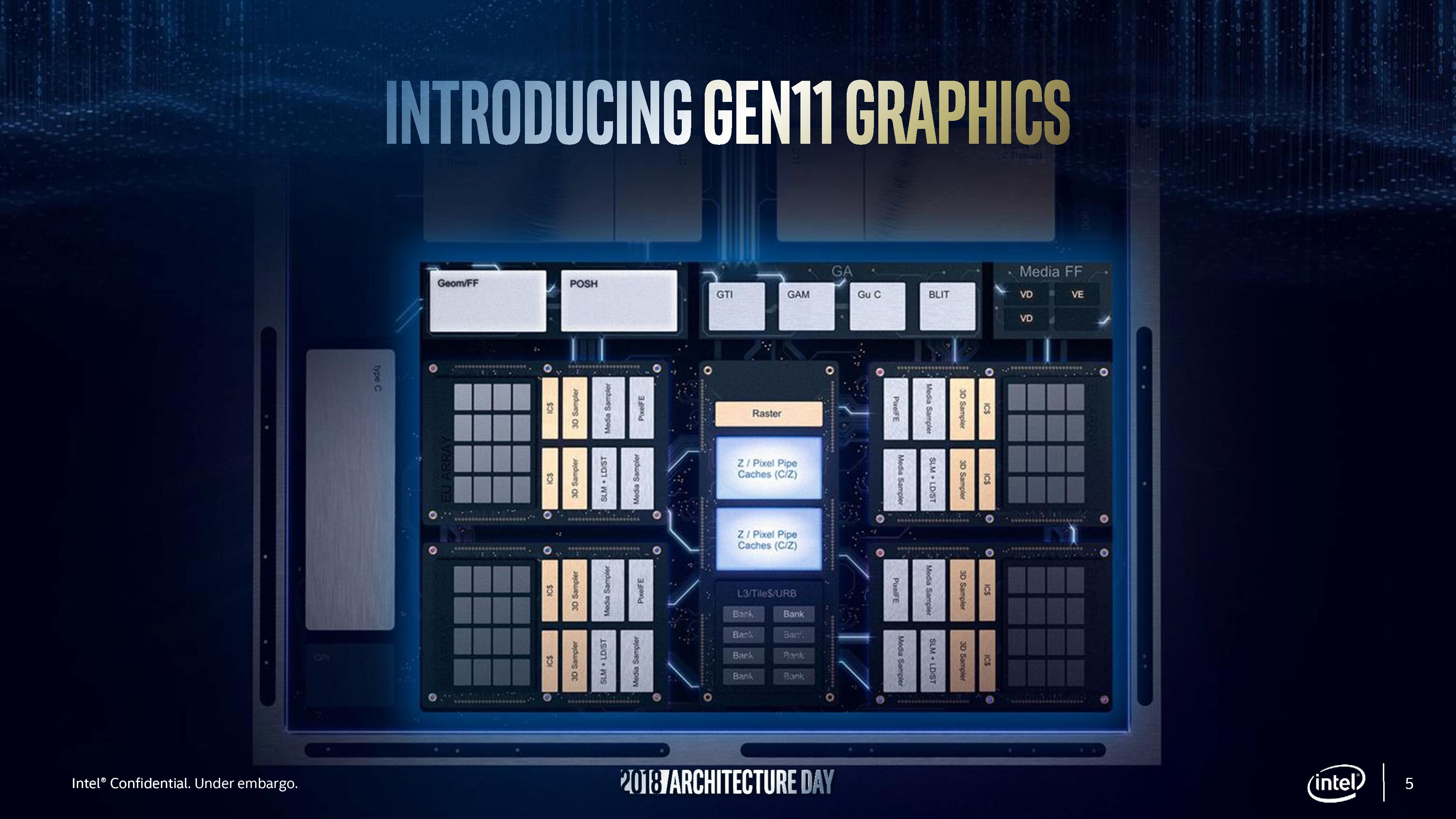
From here we can deduce a few things. We were told that this configuration is the GT2 config, which will have 64 execution units, up from 24 in Gen9.5. These 64 EUs are split into four slices, with each slice being made of two sub-slices of 8 EUs a piece. Each sub-slice will have an instruction cache and a 3D sampler, while the bigger slice gets two media samplers, a PixelFE, and additional load/store hardware. Intel lists Gen11 targeting efficiency, performance, advanced 3D and media capabilities, and a better gaming experience.
Intel didn’t go into too much detail regarding how the EUs are at higher performance, however the company did say that the FPU interfaces inside the EU are redesigned and it still has support for fast (2x) FP16 performance as seen in Gen9.5. Each EU will support seven threads as before, which means that the entire GT2 design will essentially have 512 concurrent pipelines. In order to help feed these pipes, Intel states that it has redesigned the memory interface, as well as increasing the L3 cache of the GPU to 3 MB, a 4x increase over Gen9.5, and it is now a separate block in the unslice section of the GPU.
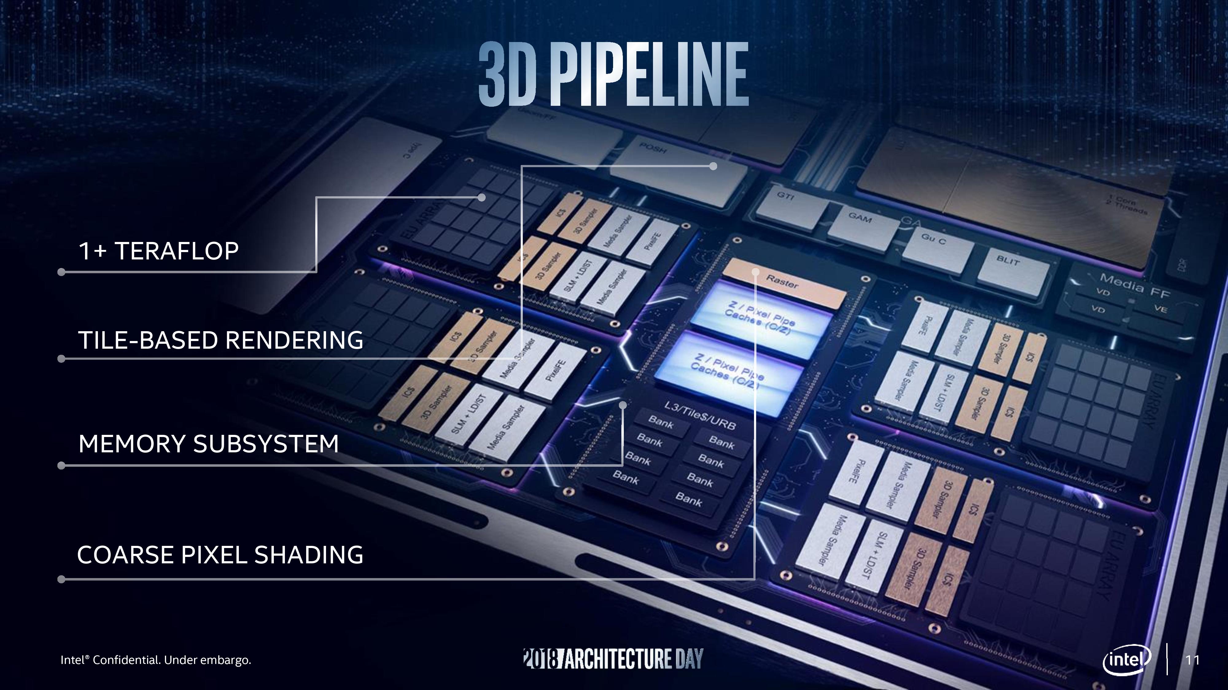
Other features include tile-based rendering, which Intel stated the graphics hardware will be able to enable/disable on a render pass basis. This will make Intel the final member of the PC GPU vendor community to implement this, following NVIDIA in 2014 and AMD in 2017. While not a panacea to all performance woes, a good tile rendering setup plays well to the bandwidth limitations of an integrated GPU. Meanwhile Intel's lossless memory compression has also improved, with Intel listing a best case performance boost of 10% or a geometric mean boost of 4%. The GTI interface now supports 64 bytes per clock read and write to increase throughput, which works with the better memory interface.
Coarse Pixel Shading, Intel's implementation of multi-rate shading and similar in scope to NVIDIA’s own Variable Pixel Shading, is also supported. This allows the GPU to reduce the amount of total shading work required by shading some pixels on a less than 1:1 basis. Intel showed two demos for CPS, where pixel shading was reduced either as a function of object distance from camera (so you do less work when things are further away), or reduced as a function of how close the object is to the center of the screen, designed to help features like foveated rendering for VR. With a 2x2 pixel stencil applied – meaning only one pixel shading operation was done per block of 4 pixels – Intel stated a ~30% increase in frame rates in supported games. Unfortunately this needs to be applied on a game-by-game basis in order to prevent significant image quality losses, so the performance gains won't be immediate or universal.
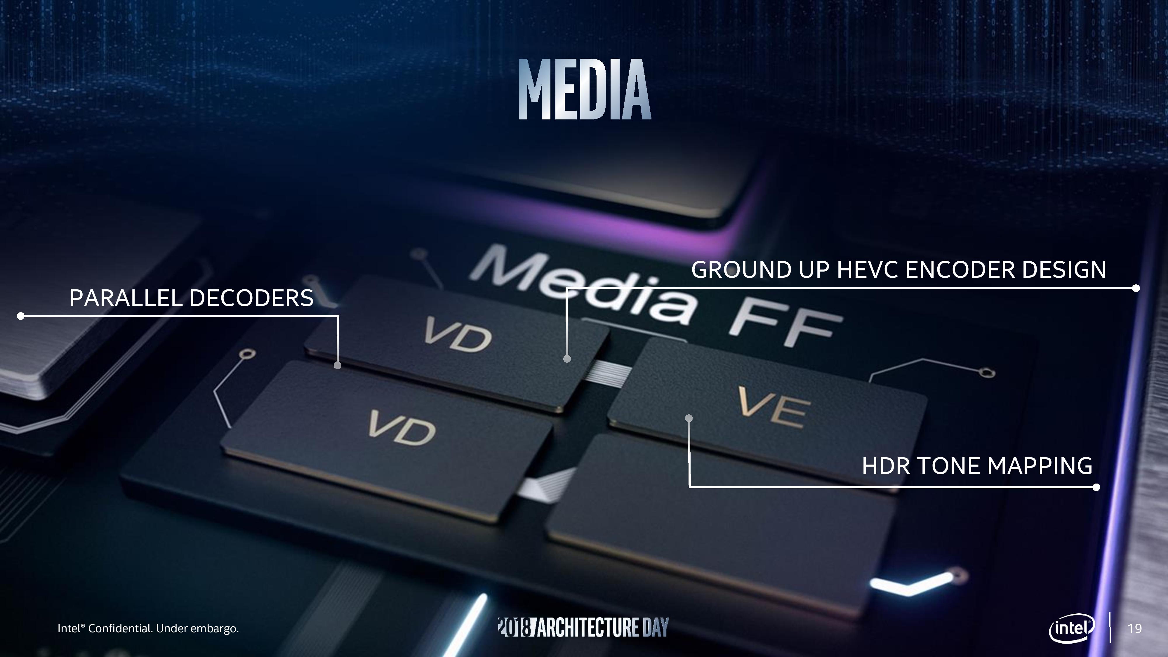
For the media block, Intel says that the Gen11 design includes a ground up HEVC encoder design, with high quality encode and decode support. Intel cited the fact that its media fixed function units are already used in the datacenter for video processing, and home users can take advantage of the same hardware. Intel also stated that by using parallel decoders it can either support concurrent video streams or they can be combined to support a single large stream, and this scalable design will allow future hardware to push the peak resolutions up to 8K and beyond.

The highlight of the display engine is support for Adaptive Sync technologies. We were told that it was announced back at the launch of Skylake, but now it is finally ready to go into Intel’s integrated graphics. This goes in hand with HDR support due to its high-precision data path.
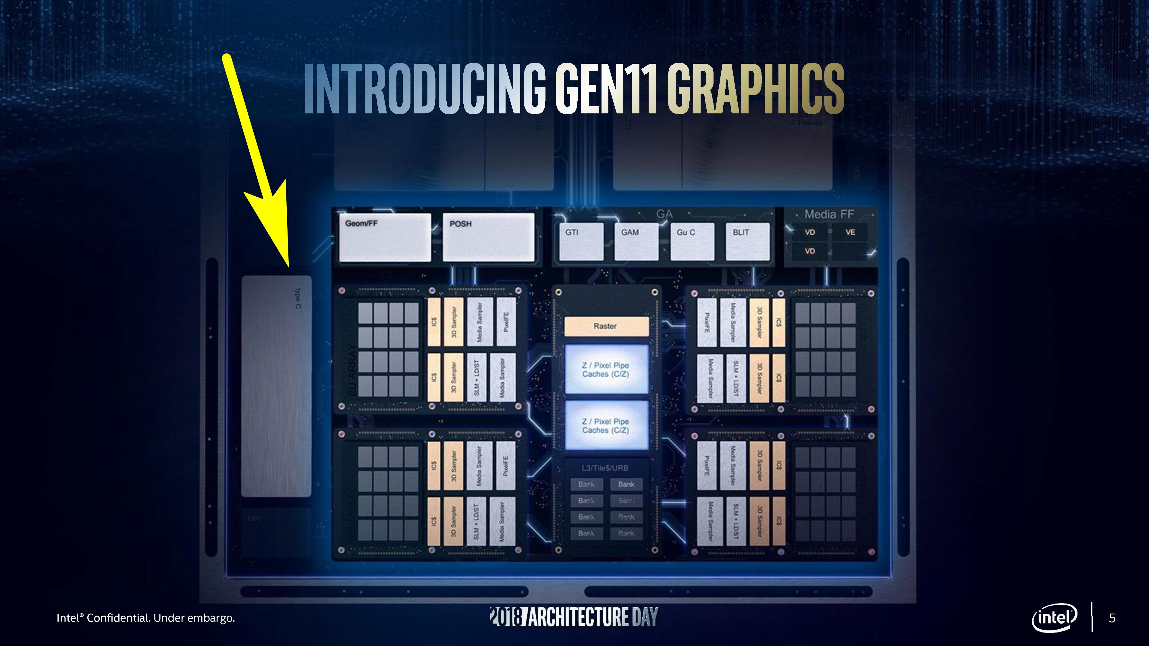
One thing in this presentation that Intel didn’t mention directly is that Gen11 graphics would appear to have Type-C video output support, potentially indicating that Intel has integrated the necessary mux into the chipset itself, removing another IC from the motherboard design.


148 Comments
View All Comments
Spunjji - Thursday, December 13, 2018 - link
They committed to Adaptive Sync back with Skylake, but it's taken this long to see it because they haven't released a new GPU design since then. It would have been a *very* weird move to suddenly release their own tech.gamerk2 - Thursday, December 13, 2018 - link
I think it's more likely NVIDIA just waits for HDMI 2.1, which supports VRR as part of the specification.I also suspect HDMI 2.1 will eventually kill of Displayport entirely; Now that HDMI offers more bandwidth, and given Displayport is a non-factor in the consumer (TV) market, there really isn't a compelling reason for it to continue to exist alongside HDMI. We *really* don't need competing digital video connector standards, and HDMI isn't going anywhere.
edzieba - Thursday, December 13, 2018 - link
HDMI is fantastic for AV, but has NO PLACE WHATSOEVER for desktop monitors. It causes a multitude of problems due to abusing a standard intended for very specific combinations of resolutions and refresh rates (and a completely different colour range and colour space standards), add offers zero benefits. Get it the hell off the back of my GPU where it wastes space that could be occupied by a far more useful DP++ connectorIcehawk - Thursday, December 13, 2018 - link
Setting all else aside - DP is "better" because the plugs lock IMO. HDMI and mini-DP both have no retention system and that makes it something I do my best to avoid both personally and professionally, love the "my monitor doesn't work" calls when it's just you moved your dock and it wiggled the mini-DP connector.jcc5169 - Wednesday, December 12, 2018 - link
Intel will be at a perpetual disadvantage because byt the time they bring our 7nm product, AMD will have been delivering for 2 whole years.shabby - Wednesday, December 12, 2018 - link
You belive tsmc's 7nm is equal to Intel's 7nm?silverblue - Wednesday, December 12, 2018 - link
7nm != 7nm in this case; in fact, Intel's 10nm process looks to be just as dense as TSMC's 7nm. I think the question is more about how quickly TSMC/GF/Samsung can offer a 5nm process, because I wouldn't expect a manufacturing lead anytime soon (assuming 10nm processors come out on time).YoloPascual - Wednesday, December 12, 2018 - link
10nm iNTeL iS bEttER tHAn 7nm TSMC???ajc9988 - Wednesday, December 12, 2018 - link
The nodes are marketing jargon. Intel's 10nm=TSMC 7nm for intents and purposes. Intel's 7nm=TSMC5n/3nm, approximately. TSMC is doing volume 5nm EUV next year, IIRC, for Apple during H2, while working on 7nm EUV for AMD (or something like that) with 5nm being offered in 2020 products alongside 7nm EUV. Intel's current info shows 7nm for 2021 with EUV, but that is about the time that TSMC is going to get 3nm, alongside Samsung which is keeping up on process roughly alongside TSMC. Intel will never again have a lead like they had. They bet on EUV and partners couldn't deliver, then they just kept doing Skylake refreshes instead of porting designs back to 14nm like the one engineer said he told them to do and Intel didn't listen.I see nothing ground breaking from Intel unless they can solve the Cobalt issues, as due to the resistances at the size of the connections at the smaller nodes, Cobalt is a necessity. TSMC is waiting to deal with Cobalt, same with Samsung, while Intel uses that and Ruthenium. Meanwhile, Intel waited so long on EUV to be ready, they gave up waiting and instead are waiting for that to mature while TSMC and Samsung are pushing ahead with it, even with the known mask issues and pellicles not being ready. The race is fierce, but unless someone falters or TSMC and Samsung can't figure out Cobalt or other III-V materials when Intel cracks the code, no one will have a clear lead by years moving forward. And use of an active interposer doesn't guarantee a clear lead, as others have the tech (including AMD) but have chosen not to use it on cost basis to date. Intel had to push chipsets back onto 22nm plants that were going to be shut down. Now that they cannot be shut down, keeping them full to justify the expense is key, and 22nm active interposers on processes that have been around the better part of the last decade (high yield, low costs due to maturity) is a good way to achieve that goal. In fact, producing at 32nm and below, in AMD's cost analysis, shows that the price is the same as doing a monolithic die. That means, since Intel never got a taste of chiplets giving better margins with an MCM, Intel won't feel a hit by going straight for the active interposer, as the cost is going to be roughly what their monolithic dies cost.
porcupineLTD - Thursday, December 13, 2018 - link
TSMC will start risc production of 5nm in late 2019 at the earliest, next apple SOC will be 7nm+(EUV) and so will zen 3.