Intel's Architecture Day 2018: The Future of Core, Intel GPUs, 10nm, and Hybrid x86
by Dr. Ian Cutress on December 12, 2018 9:00 AM EST- Posted in
- CPUs
- Memory
- Intel
- GPUs
- DRAM
- Architecture
- Microarchitecture
- Xe
Sunny Cove Microarchitecture: A Peek At the Back End
One of the best parts when a new microarchitecture is announced is learning how it all works and how it has changed. Intel has been on close variants of the Skylake core since Skylake first launched in 2015, which has carried through Kaby Lake, Coffee Lake, and Coffee Lake refresh – and so getting an update to his old core design is more than welcome. While I applaud Intel for getting something new to put in front of our faces, the level of information was unfortunately less than complete. For reasons of ‘we’ll discuss more nearer the launch’, Intel was only set on discussing the back end of the microarchitecture design in any detail. In core design parlance, this means everything beyond the dispatch and order queues.
Intel framed its microarchitecture updates into two different sections: general purpose performance increases and special purpose performance increases. The company described the general purpose updates essentially as raw IPC (instructions per clock) throughput or an increase in frequency. An increase in either of these two leads to a performance increase no matter the code, at least as long as it is compute bound. Frequency is often a function of the implementation and process, whereas IPC increases can come from cores being wider (more executing instructions per clock), deeper (more parallelism per clock), and smarter (better data delivery through the front end).

The other type of performance increase is the special purpose kind, which means that certain workloads used in specific scenarios can be improved through additional acceleration methods, such as dedicated IP or specialized instructions.
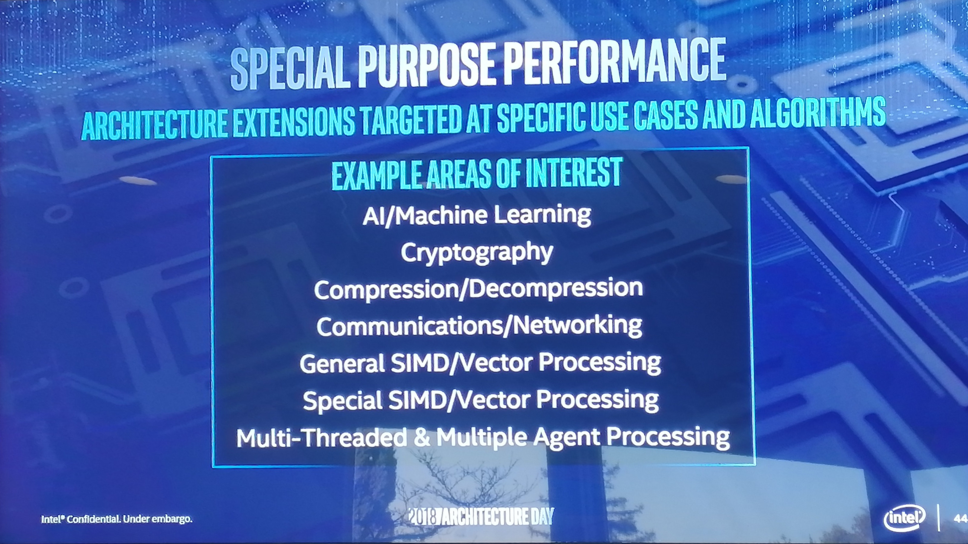
Sunny Cove is set to have both.
On the back end of the microarchitecture design, Intel has done several things including increasing cache sizes, making the execution of the core wider, increasing L1 store bandwidth, and other things.
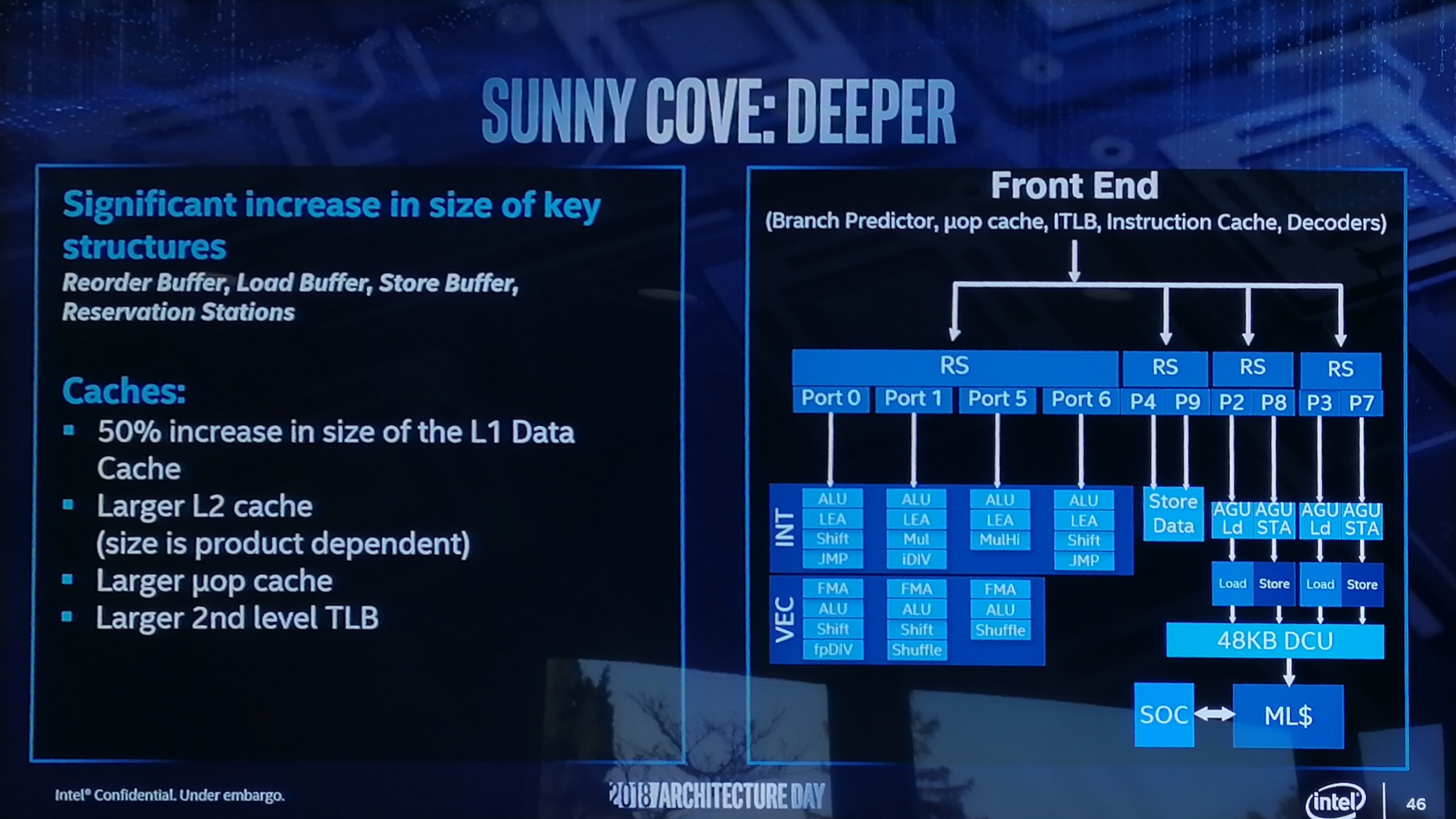
Starting with the cache improvements, the Sunny Cove core back end has a 48 KB L1 Data cache, upgraded from 32 KB. Normally cache misses decrease by a factor of a square root of the proportional size when the cache is increased, so in this case we should expect a 22% reduction in L1-Data cache misses. We are told that the L2 cache size has also been increased in both the Core and Xeon variants of Sunny Cove (256 KB and 1 MB respectively), although to exactly what size will be revealed at a later date.
While not back-end, the micro-op (uOp) cache has increased from a 2048-entry design, although exactly to what Intel is not saying at this point. The second level TLB size has also increased, which will help with machine address translation of recent addresses – normally this is increased when more lookups need to be kept and stored, which means that Intel identified a number of use cases where recent addresses had been evicted shortly before being needed.

From the diagram we can see some other changes, such as the increase in execution ports from eight to ten, allowing more instructions to come out of the schedulers at one time. Port 4 and Port 9 is linked to a cycling data store, doubling that bandwidth, but also the AGU store capabilities have doubled, for which the increased L1-D size will help. Previously on Skylake there was a potential bottleneck when all three AGUs could attempt a store, however only enough bandwidth was present for one per clock cycle. Load performance is unaffected. There is also an allocation increase, moving from four to five. This means that the dispatch out of the reorder buffer can now hit five instructions per cycle, rather than four – however given that the ops/cycle out of the Skylake decoders and uOp cache was four-to-five (depending on certain factors), it will be interesting to see how the front end has changed as a result.
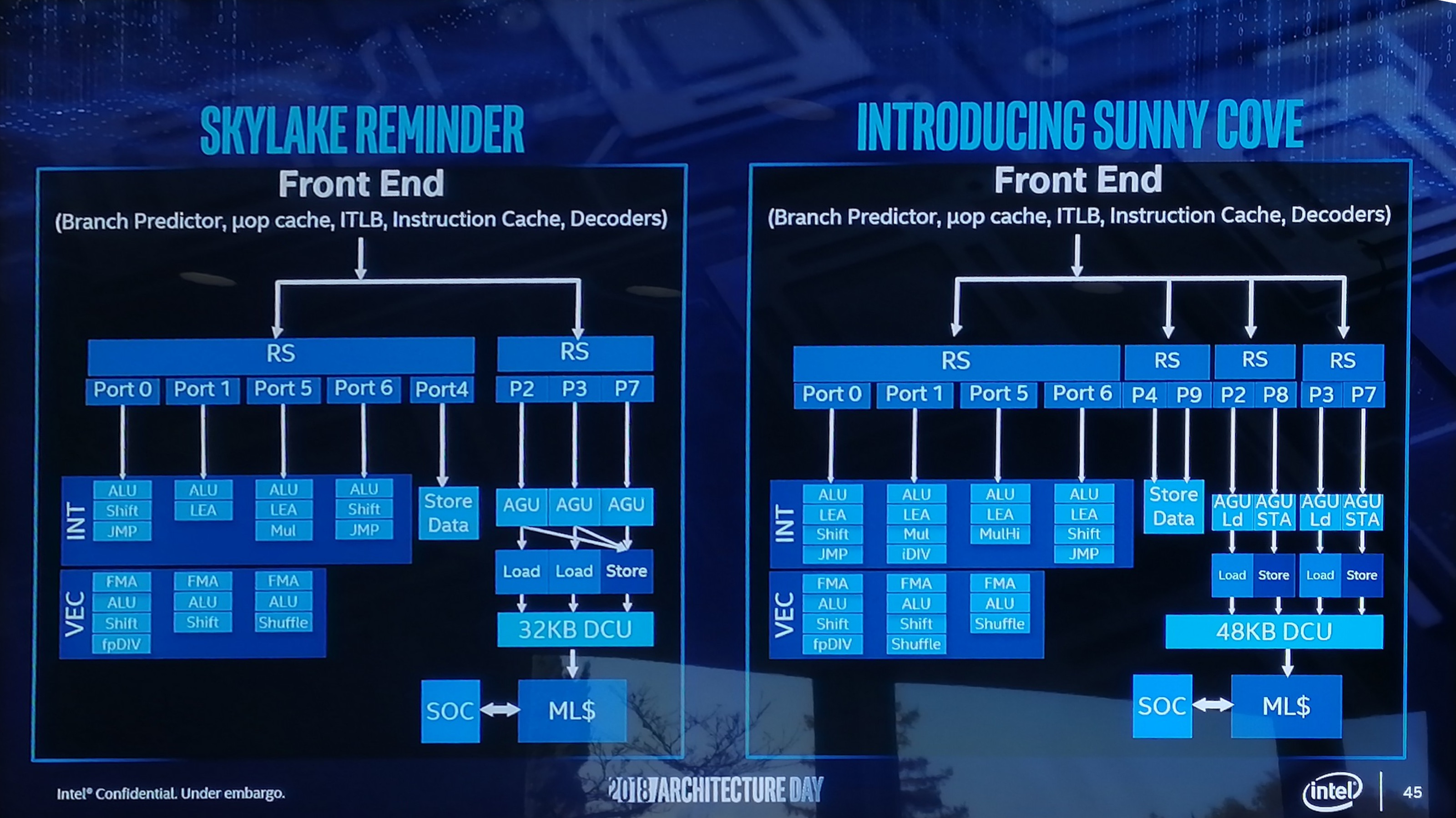
There are also substantial changes in the execution ports between Skylake and Sunny Cove, which is best represented in a diagram and a table:
| Back-End Execution Resources | ||||||||
| Skylake | Port | Sunny Cove | ||||||
| Integer | ||||||||
| JMP | Shift | ALU | 0 | ALU | LEA | Shift | JMP | |
| LEA | ALU | 1 | ALU | LEA | Mul | iDIV | ||
| Mul | LEA | ALU | 5 | ALU | LEA | MulHi | ||
| JMP | Shift | ALU | 6 | ALU | LEA | Shift | JMP | |
| Vector / FP | ||||||||
| fpDIV | Shift | ALU | FMA | 0 | FMA | ALU | Shift | fpDIV |
| Shift | ALU | FMA | 1 | FMA | ALU | Shift | Shuffle | |
| Shuffle | ALU | FMA | 5 | FMA | ALU | Shuffle | ||
The parts highlighted in bold are different in the Sunny Cove core.
We see that Intel has equipped the Integer section of the core with more LEA units to help with memory addressing calculations, possibly to help improve performance loss with security mitigations that require frequent memory calculations or to help with high-performance array code with constant offsets. Port 1 gets the Mul unit from Skylake Port 5, probably for rebalancing purposes, but there is also an integer divider unit here. This addition is a bit of a tweak, as we know that Cannon Lake has a 64-bit IDIV unit in its design as well. In that case it brings 64-bit integer division down from 97 clocks (a mix of instructions) down to 18 clocks, and this is likely something similar. Also on the INT side is that Port 5’s multiply unit has become a ‘MulHi’ unit which in other implementations leave most-significant nibble of the result in a register for further use. I'm not sure exactly what its position is here in the Sunny Cove core though.
On the FP side, Intel has increased the shuffle resources, which we are told was because they had customers requesting this functionality to help remove bottlenecks in their code. Intel didn’t state the capabilities for the FMAs in the FP part of the core, however we do know that the core has an AVX-512 unit, so at least one of these FMAs should interface with it. Cannon Lake only has one 512-bit FMA, and that most likely carries over here, and the Xeon Scalable version might get two. I would like to get proved wrong though.
Other updates to the core as listed from Intel include improvements to the branch predictor and a reduced ‘effective load latency’ (due to the TLB and L1-D), although it was pointed out that these improvements won’t help everyone, and might require new algorithms in order to use specific parts of the core.
We’re waiting to see what changes Intel has made on the front-end, which is where a lot of low-hanging fruit often lies for performance.
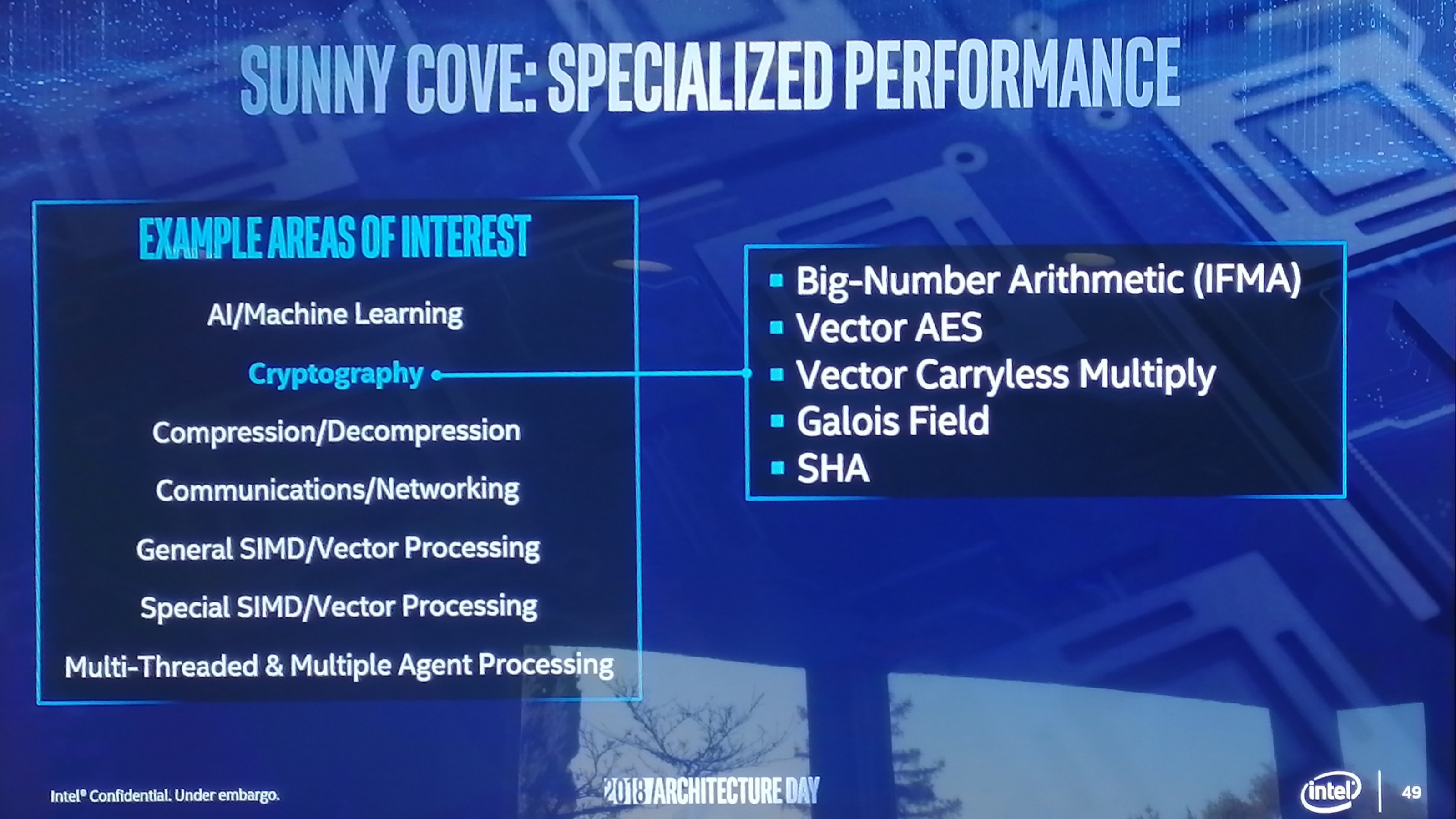
On top of the microarchitecture differences, there are new instructions for the Sunny Cove core to help speed up specialist compute tasks. With the AVX-512 unit in play, the new core will support IFMA instructions for big arithmetic compute, and which are also useful in cryptography. Along the same lines, Vector-AES (supporting more AES concurrently) and Vector Carryless Multiply are also supported. SHA and SHA-NI instructrions are also added, along with Galois Field instructions, which are fundamental building blocks in some elements of cryptography as well.
For Sunny Cove, there is also built-in support for larger memory capacities. The paging table for main memory is now a five layer design, up from four layers, supporting a Linear Address space up to 57 bits and a physical address space up to 52 bits. This means, according to Intel, that the server processors could theoretically support 4 TB of memory per socket. We will see Sunny Cove hit the market in the server space with Ice Lake-SP in 2020 according to Intel’s previous Xeon roadmaps. For security, Sunny Cove has access to Multi-Key Total Memory Encryption, and User Mode Instruction Prevention.
So where does this leave us in terms of Sunny Cove predicted performance compared to Skylake at a clock for clock level? Unfortunately we don’t have enough information. There is only enough to whet the appetite. Intel wants you (and me) to come back for more in 2019.


148 Comments
View All Comments
Spunjji - Thursday, December 13, 2018 - link
They committed to Adaptive Sync back with Skylake, but it's taken this long to see it because they haven't released a new GPU design since then. It would have been a *very* weird move to suddenly release their own tech.gamerk2 - Thursday, December 13, 2018 - link
I think it's more likely NVIDIA just waits for HDMI 2.1, which supports VRR as part of the specification.I also suspect HDMI 2.1 will eventually kill of Displayport entirely; Now that HDMI offers more bandwidth, and given Displayport is a non-factor in the consumer (TV) market, there really isn't a compelling reason for it to continue to exist alongside HDMI. We *really* don't need competing digital video connector standards, and HDMI isn't going anywhere.
edzieba - Thursday, December 13, 2018 - link
HDMI is fantastic for AV, but has NO PLACE WHATSOEVER for desktop monitors. It causes a multitude of problems due to abusing a standard intended for very specific combinations of resolutions and refresh rates (and a completely different colour range and colour space standards), add offers zero benefits. Get it the hell off the back of my GPU where it wastes space that could be occupied by a far more useful DP++ connectorIcehawk - Thursday, December 13, 2018 - link
Setting all else aside - DP is "better" because the plugs lock IMO. HDMI and mini-DP both have no retention system and that makes it something I do my best to avoid both personally and professionally, love the "my monitor doesn't work" calls when it's just you moved your dock and it wiggled the mini-DP connector.jcc5169 - Wednesday, December 12, 2018 - link
Intel will be at a perpetual disadvantage because byt the time they bring our 7nm product, AMD will have been delivering for 2 whole years.shabby - Wednesday, December 12, 2018 - link
You belive tsmc's 7nm is equal to Intel's 7nm?silverblue - Wednesday, December 12, 2018 - link
7nm != 7nm in this case; in fact, Intel's 10nm process looks to be just as dense as TSMC's 7nm. I think the question is more about how quickly TSMC/GF/Samsung can offer a 5nm process, because I wouldn't expect a manufacturing lead anytime soon (assuming 10nm processors come out on time).YoloPascual - Wednesday, December 12, 2018 - link
10nm iNTeL iS bEttER tHAn 7nm TSMC???ajc9988 - Wednesday, December 12, 2018 - link
The nodes are marketing jargon. Intel's 10nm=TSMC 7nm for intents and purposes. Intel's 7nm=TSMC5n/3nm, approximately. TSMC is doing volume 5nm EUV next year, IIRC, for Apple during H2, while working on 7nm EUV for AMD (or something like that) with 5nm being offered in 2020 products alongside 7nm EUV. Intel's current info shows 7nm for 2021 with EUV, but that is about the time that TSMC is going to get 3nm, alongside Samsung which is keeping up on process roughly alongside TSMC. Intel will never again have a lead like they had. They bet on EUV and partners couldn't deliver, then they just kept doing Skylake refreshes instead of porting designs back to 14nm like the one engineer said he told them to do and Intel didn't listen.I see nothing ground breaking from Intel unless they can solve the Cobalt issues, as due to the resistances at the size of the connections at the smaller nodes, Cobalt is a necessity. TSMC is waiting to deal with Cobalt, same with Samsung, while Intel uses that and Ruthenium. Meanwhile, Intel waited so long on EUV to be ready, they gave up waiting and instead are waiting for that to mature while TSMC and Samsung are pushing ahead with it, even with the known mask issues and pellicles not being ready. The race is fierce, but unless someone falters or TSMC and Samsung can't figure out Cobalt or other III-V materials when Intel cracks the code, no one will have a clear lead by years moving forward. And use of an active interposer doesn't guarantee a clear lead, as others have the tech (including AMD) but have chosen not to use it on cost basis to date. Intel had to push chipsets back onto 22nm plants that were going to be shut down. Now that they cannot be shut down, keeping them full to justify the expense is key, and 22nm active interposers on processes that have been around the better part of the last decade (high yield, low costs due to maturity) is a good way to achieve that goal. In fact, producing at 32nm and below, in AMD's cost analysis, shows that the price is the same as doing a monolithic die. That means, since Intel never got a taste of chiplets giving better margins with an MCM, Intel won't feel a hit by going straight for the active interposer, as the cost is going to be roughly what their monolithic dies cost.
porcupineLTD - Thursday, December 13, 2018 - link
TSMC will start risc production of 5nm in late 2019 at the earliest, next apple SOC will be 7nm+(EUV) and so will zen 3.